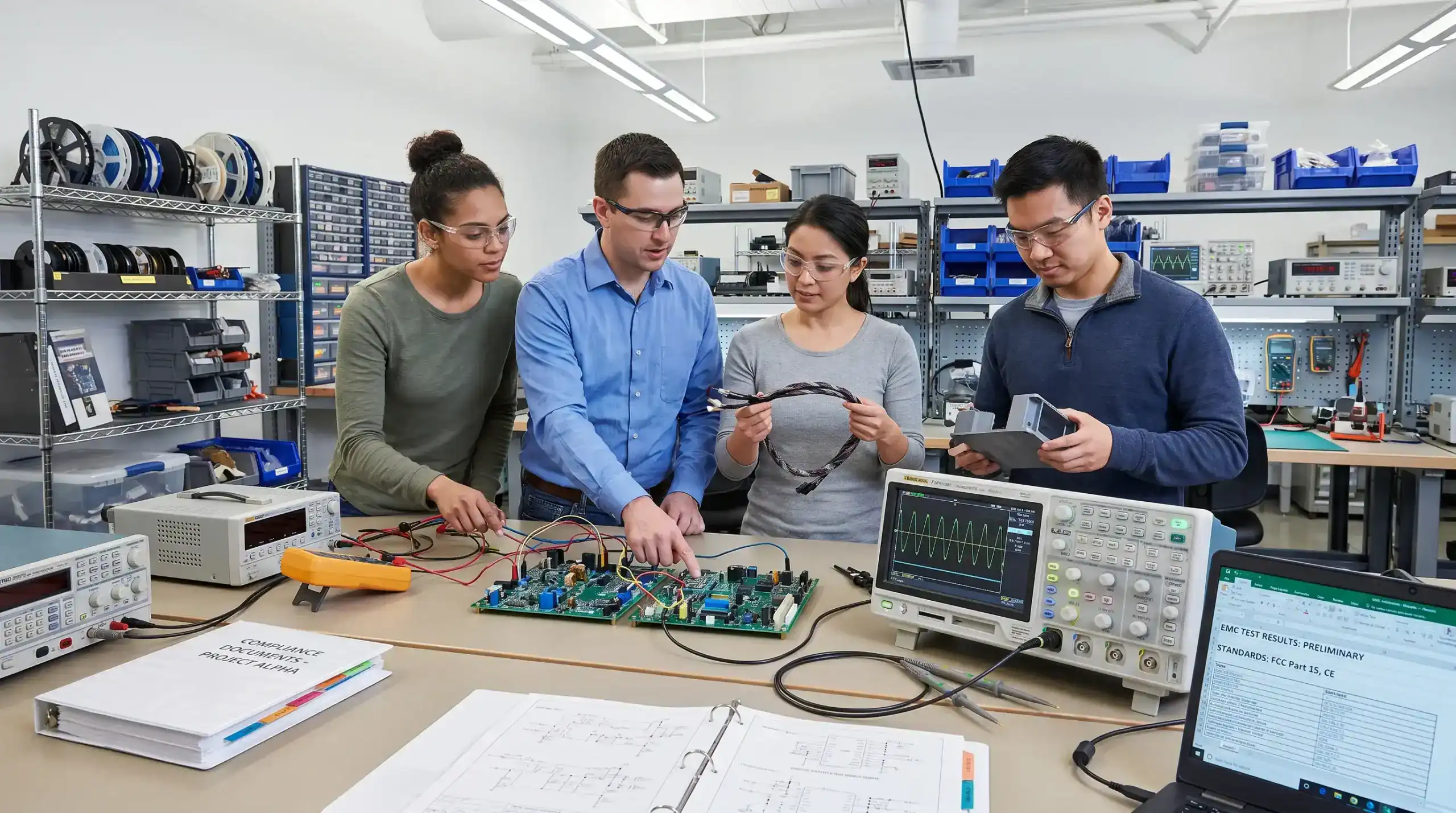
Product launches rarely slip because one assembly step takes longer than expected. More often, delays come from a chain of small decisions made earlier in the design, sourcing and test process. A footprint that almost fits. A component that was acceptable for a lab prototype but unavailable for production. A test point that seemed unnecessary until the first failed batch had to be debugged by hand.
For OEMs building high-value machines, embedded products, defence systems, maritime equipment, robotics or connected devices, PCB manufacturing assembly is not a purchasing formality. It is part of the engineering process. When manufacturing and assembly constraints are considered too late, the result is rework, unclear responsibilities, repeated prototypes, certification uncertainty and lost launch momentum.
Below are the most common PCB manufacturing assembly mistakes that slow product launch, and how engineering teams can prevent them before they become expensive schedule risks.
Why PCB manufacturing assembly mistakes create more than production delays
A PCB assembly issue is rarely isolated to the assembly line. It can affect enclosure fit, firmware bring-up, EMC behaviour, thermal performance, field reliability, serviceability and compliance documentation. In complex products, these dependencies are tightly connected.
A prototype that works on the bench may still be difficult to manufacture consistently. It may need manual soldering, non-standard inspection, fragile connectors, late component substitutions or unclear programming steps. Each exception increases handling time and creates variation. Variation then makes root-cause analysis harder when a board fails during test, certification or field trials.
This is why launch readiness must be treated as a system-level concern. The board, embedded software, power electronics, sensors, cables, enclosure and manufacturing process all need to be aligned. A supplier can assemble what is specified, but if the specification is incomplete or based on assumptions, the assembly result can expose weaknesses that were already built into the product.
Mistake 1: treating assembly as a late-stage procurement task
One of the most damaging mistakes is involving the assembly partner only after the PCB layout is finished. At that point, many decisions are already locked in: stack-up, component spacing, thermal relief, soldering process, panelisation, fiducials, test access and connector orientation.
If the assembler then identifies a manufacturability issue, the team may face a difficult choice. Either accept a risky build with manual workarounds, or return to layout changes and lose time. Neither option is ideal close to launch.
Manufacturing input should be part of design reviews before release. This does not mean the assembler controls the design. It means the engineering team validates whether the design can be built repeatedly, inspected properly and tested efficiently. For more detail on how early choices influence build quality, ProMicro’s guide to PCB fabrication and assembly choices explains the relationship between technical design decisions and lifecycle performance.
Mistake 2: releasing an incomplete manufacturing data package
A PCB assembly package is more than Gerber files and a bill of materials. When the manufacturing data is incomplete, the assembler must interpret missing information. That interpretation can introduce delays, questions, incorrect assumptions or inconsistent builds.
A production-ready package usually needs clear revision control, fabrication data, assembly drawings, BOM with manufacturer part numbers, placement files, polarity markings, special handling notes, programming requirements and inspection criteria. For products with safety, EMC or environmental constraints, additional notes may be needed around creepage, clearance, insulation, coating, torque, shielding, thermal interfaces and approved alternatives.
The issue is not only whether the data exists. It must also be coherent. A mismatch between schematic revision, PCB layout, BOM and firmware version can cost days before anyone even starts solving the actual technical problem.
| Missing or unclear item | Typical consequence | Better practice |
|---|---|---|
| Uncontrolled BOM substitutions | Electrical behaviour changes without review | Define approved alternates and approval workflow |
| Ambiguous polarity markings | Incorrect component orientation or inspection delays | Make polarity clear in silkscreen, drawings and assembly notes |
| No programming instruction | Boards wait for engineering support | Include firmware version, connector method and verification step |
| Poor revision control | Wrong files used for build or test | Use a controlled release package with traceable revisions |
| No test criteria | Pass or fail decisions become subjective | Define measurable acceptance limits before build |
Mistake 3: designing for a prototype process, then expecting volume behaviour
Prototype builds often tolerate manual effort. An engineer can rework a connector, hand-solder a difficult component, add a wire modification or test each board slowly. That can be acceptable for learning, but it is not a scalable manufacturing strategy.
Problems appear when the same design is pushed directly towards launch. Manual operations increase cost, lead time and variation. They also make it harder to prove that the product can be built consistently over time. In regulated or demanding markets, this can affect traceability and reliability confidence.
The transition from prototype to production should be planned deliberately. The team should ask whether the assembly process used for prototypes reflects the intended production process. If not, the prototype must be understood as an engineering learning step, not evidence that the product is production-ready. ProMicro’s article on printed circuit board assembly from prototype to volume covers this transition in more depth.
Mistake 4: underestimating component availability and lifecycle risk
Component choices can slow launch long before a board reaches the assembly line. A design may depend on a component with long lead times, limited distributor availability, uncertain lifecycle status or a package that is difficult to source in the required quantity. This is especially relevant in embedded systems, power electronics, wireless modules and analogue front ends, where substitutions are rarely simple drop-in changes.
Late substitutions can affect EMC behaviour, thermal performance, firmware compatibility, calibration, accuracy, power consumption and certification evidence. Even a passive component change can matter in high-frequency, precision analogue or safety-related parts of the circuit.
A stronger approach is to evaluate supply-chain risk during component selection. Critical components should have lifecycle status checks, second-source options where technically realistic and clear rules for alternative approval. If a part is unique, high-risk or strategically important, the team should recognise that early and plan procurement accordingly.
Mistake 5: ignoring design for test until failures appear
Testing is often treated as something that happens after assembly. In reality, testability is designed into the PCB. If there are no useful test points, no accessible programming connector, no boundary-scan strategy and no defined functional test method, every failure becomes harder to investigate.
This is particularly costly during launch, when the team needs fast feedback. Without clear diagnostics, a failed board may require manual probing, engineering judgement and time-consuming comparison with working units. If several boards fail in different ways, the launch team can lose confidence in both the design and the manufacturing process.
Design for test does not always require a complex automated fixture at the first prototype stage. It does require thinking ahead. Critical rails, communication buses, reset lines, programming interfaces, sensor signals and safety-relevant nodes should be accessible enough to support bring-up, debugging and production verification.
A practical test strategy should define what must be verified at bare board level, after assembly, after programming and after integration into the final product. It should also define what evidence is needed for release decisions.
Mistake 6: separating PCB layout from EMC, thermal and power integrity decisions
A layout can pass a basic design-rule check and still be unsuitable for reliable operation. This is common in products with motor drives, switching power supplies, wireless communication, sensors, long cables or sensitive analogue measurements.
If high-current paths, return currents, grounding strategy, shielding, creepage, clearance, thermal dissipation and connector placement are not handled correctly, the assembled board may work only under ideal lab conditions. Problems then appear during EMC pre-compliance, environmental testing, machine integration or field trials.
These failures are painful because they often require layout changes, enclosure changes, filter changes or firmware adjustments. They may also trigger questions about whether previous test results are still valid.
Good PCB manufacturing assembly planning therefore includes electrical performance, not only solderability. The assembly process must support the intended design, but the design must also support stable real-world behaviour. For complex products, this requires collaboration between hardware engineers, embedded software developers, mechanical designers and manufacturing specialists.
Mistake 7: overlooking mechanical integration and enclosure constraints
Boards are not used in isolation. They sit inside enclosures, connect to cables, dissipate heat, experience vibration and are handled by operators or service engineers. Assembly mistakes often start when the PCB is designed without enough consideration for this physical environment.
Connector placement may look logical in CAD but be difficult to access in the enclosure. A tall component may interfere with the housing. A heat-generating device may sit too close to a plastic wall. A cable may force mechanical stress onto a solder joint. A conformal coating requirement may conflict with connectors or test pads.
These issues can delay launch because they often appear during system integration, not during bare PCB assembly. By then, the enclosure, cable harness and board layout may all need adjustment.
Mechanical integration should be reviewed early with realistic use cases. That includes assembly sequence, service access, vibration, sealing, thermal paths, connector mating, operator safety and environmental exposure. In professional products, these details are not cosmetic. They influence reliability and liability.
Mistake 8: changing the design without disciplined change control
Late changes are normal in product development. The problem is not change itself, but uncontrolled change. When BOM items, PCB revisions, firmware versions, test procedures and mechanical parts move independently, the team can lose track of what was built, tested and approved.
This creates launch delays because every unexpected result becomes harder to interpret. Did the board fail because of the new layout, the changed component, the updated firmware or a manufacturing variation? Without traceability, engineering time is spent reconstructing history instead of solving the problem.
A controlled engineering change process should connect the reason for the change, affected documents, validation evidence and release decision. This is especially important when moving from prototype batches to pilot production and volume manufacturing.
Cross-functional teams can learn from structured decision-making methods used outside engineering. For example, business simulation software is often used to make strategy and innovation trade-offs visible in a low-risk environment. Electronics teams need a similar mindset during launch preparation: decisions should be tested against realistic constraints before they reach the production floor.
Mistake 9: choosing an assembly route on price alone
Cost matters, but the cheapest quotation is not always the lowest-risk route to launch. A technically weak assembly route can create hidden costs through repeated questions, rejected boards, slow debugging, poor documentation, rework or inability to scale.
The right assembly route depends on product complexity and risk. A simple board with standard components may not need the same level of engineering interaction as a power electronics controller, wireless embedded device or safety-relevant machine module. But for complex products, the assembler’s capability, process control, inspection methods, technical communication and willingness to handle controlled changes are critical.
Engineering leaders should evaluate whether the assembly partner can support the intended production maturity, not just the next batch. This includes questions around traceability, inspection, rework control, moisture-sensitive components, programming, test fixtures, documentation and feedback loops to design engineering.
Mistake 10: assuming compliance can be fixed after assembly
Compliance-related delays often appear late, but their causes are usually early. EMC, RED, CE, safety and environmental requirements can influence architecture, layout, shielding, filtering, component selection, firmware behaviour, enclosure design and documentation.
If these requirements are treated as a final checkbox, the assembled board may need redesign after pre-compliance or certification testing. That can affect not only the PCB, but also cables, enclosure openings, antennas, grounding, power supply behaviour and software states.
Designing with compliance in mind does not guarantee a first-pass approval, and responsible engineering teams should avoid that assumption. It does, however, reduce avoidable risk. Requirements should be translated into design constraints early, then verified progressively through reviews, measurements and pre-compliance testing where appropriate. ProMicro has also written about embedded system design mistakes that delay certification, which is closely related to PCB launch readiness.
How to prevent assembly mistakes before they slow launch
Preventing PCB manufacturing assembly delays is less about one final checklist and more about disciplined engineering collaboration. The most effective teams build manufacturability, testability, compliance and lifecycle thinking into the project from the beginning.
A useful launch-readiness review should cover these areas:
- Requirements: operating environment, safety constraints, user context, compliance targets and service expectations are clearly defined.
- Design data: PCB files, BOM, drawings, firmware and test procedures are complete, consistent and under revision control.
- Manufacturability: component placement, soldering process, panelisation, inspection and rework constraints have been reviewed.
- Testability: critical signals, power rails, programming interfaces and functional tests are accessible and documented.
- Supply chain: critical components, lifecycle risks and approved alternatives have been assessed before release.
- Integration: enclosure, cabling, thermal paths, EMC measures and mechanical handling have been validated at system level.
This review should not wait until the product is almost ready to ship. It is most valuable before layout release, before prototype build, before pilot production and before committing to volume manufacturing.
Frequently asked questions
What is the biggest PCB manufacturing assembly mistake before launch? The biggest mistake is treating assembly as separate from product development. Assembly readiness depends on design choices, documentation, component selection, test strategy, compliance planning and system integration. If these are handled too late, launch delays become much more likely.
Can a working prototype still be unsuitable for production? Yes. A prototype can prove basic functionality while still relying on manual rework, unavailable components, poor test access or assembly methods that do not scale. Production readiness requires repeatability, documentation, controlled changes and clear acceptance criteria.
When should design for manufacturability be reviewed? It should be reviewed before PCB layout release and again before each major build stage. Early reviews prevent layout changes from becoming urgent rework after the assembler identifies issues.
How does PCB assembly affect EMC and certification risk? Assembly choices can influence grounding, shielding, component placement, cable interfaces, filtering and consistency between units. These factors affect EMC behaviour and can create certification delays if not considered during design.
Why involve an electronics design partner before selecting an assembler? A design partner can help translate product requirements into manufacturable, testable and compliance-aware electronics. This helps the team choose an assembly route that matches the technical risk of the product, not only the batch price.
Build launch readiness into the design, not after it
PCB manufacturing assembly mistakes slow product launch because they reveal design, sourcing and test weaknesses at the point where time is most limited. The best way to avoid them is to connect engineering decisions with manufacturing reality from the beginning.
ProMicro supports companies developing complex electronic products with embedded systems, power electronics, analogue electronics, PCB design, prototyping and preparation for volume manufacturing. If your team is moving from concept or prototype towards a production-ready product, speak with ProMicro about reducing technical risk before assembly issues become launch delays.