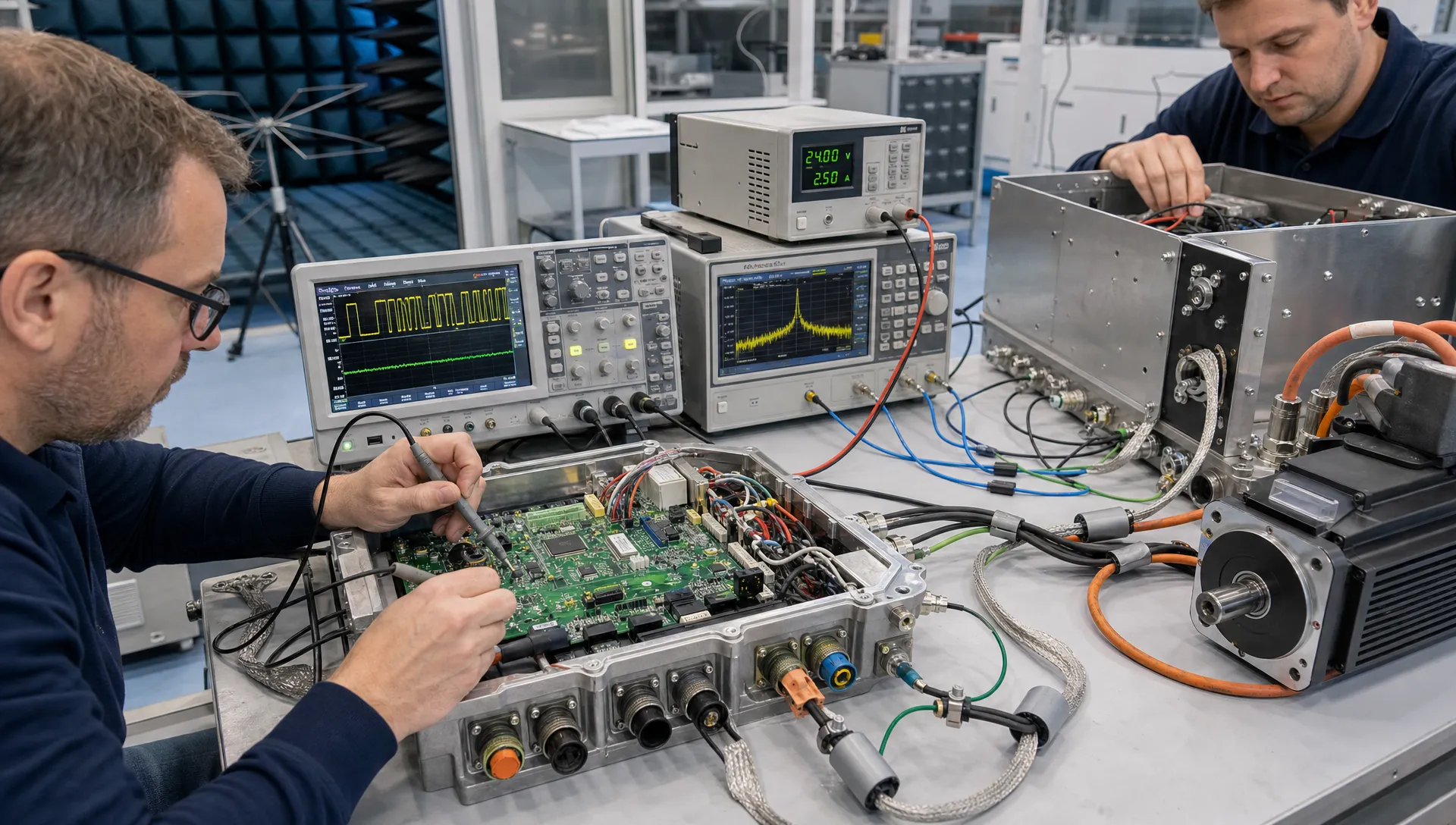
Electronics that operate in defence, maritime, high-tech, robotics, automotive or industrial environments rarely fail because of one isolated detail. They fail because energy moves through the product in ways the design did not anticipate. EMC design is the discipline of controlling that energy so the product limits unwanted emissions and remains immune to disturbances from its surroundings. For engineering managers and technical directors, this is not only a compliance topic. It is a reliability, safety, lifecycle and business-risk topic.
A prototype can appear stable on the bench and still behave unpredictably near a motor drive, radio transmitter, switching power supply, long cable harness or metal machine frame. The earlier electromagnetic compatibility is considered, the fewer late redesigns, enclosure changes and certification surprises the development team has to absorb. If you need a foundation on emissions and immunity, ProMicro’s explanation of EMC meaning in product design gives useful context before diving into the engineering principles below.
The operating environment comes before the schematic
Demanding environments should shape the electronics architecture before component selection or PCB layout begins. A product installed on a vessel, inside a mobile robot or next to a high-current industrial actuator sees a different electromagnetic world than a product used in a controlled laboratory. The same circuit can behave very differently once cable length, grounding structure, enclosure material, ambient temperature and installation behaviour are included.
For that reason, requirements work must go beyond the written specification. The development team should understand how the product is powered, where it is mounted, which other systems are nearby, what users connect to it and what fault conditions are realistic. Good EMC design starts by converting that context into design constraints, rather than treating compliance as a final laboratory exercise.
Build an electromagnetic risk profile
An electromagnetic risk profile identifies likely sources of disturbance and likely victim circuits. Sources may include switching converters, motor phases, relays, wireless modules, fast digital buses, ESD events, surge conditions and external radio fields. Victim circuits often include analogue sensor inputs, references, clock circuits, reset lines, communication interfaces and high-impedance nodes.
This profile does not need to be complicated, but it must be explicit. It helps the team make architecture decisions with purpose, such as isolating a noisy power stage, selecting a differential interface, moving an analogue front end closer to the sensor or choosing a shielded enclosure concept.
Translate use conditions into design constraints
A compliance standard describes test methods and limits, but it does not describe every real installation. Products used in professional markets often face long cable runs, shared power supplies, service modifications, condensation, vibration or proximity to high-energy equipment. These conditions affect grounding, insulation, shielding, connector selection and filtering.
The practical output should be a set of engineering constraints. Examples include maximum cable length, required surge protection, separation between power and signal harnesses, enclosure bonding strategy, service access limitations and preferred grounding concept. These constraints make later reviews more objective.
EMC design principles for system architecture
A robust architecture reduces the amount of unwanted energy that reaches sensitive circuits in the first place. This is more effective than attempting to filter, shield or patch a noisy product after the first failed test. At system level, EMC design is about partitioning functions, controlling current paths and defining interfaces so the product behaves predictably in its intended environment.
Keep noisy energy local
Every switching event creates a current loop. The larger the loop area and the faster the transition, the greater the potential for radiated and conducted interference. This is especially relevant in power electronics, motor control, LED drivers, solenoid drivers and fast digital circuits.
The design goal is to keep high di/dt and high dv/dt energy close to its source. That affects component placement, capacitor selection, loop geometry, snubber design, gate-drive behaviour and the physical relationship between power stages and control electronics. If a noisy function has to be present, it should be contained rather than allowed to travel through the entire system.
Separate functions by behaviour, not only by board area
A common mistake is to divide a PCB visually rather than electromagnetically. The important question is not only where circuits fit, but how they behave. High-current switching, precision analogue sensing, radio communication, microcontroller logic and external I/O each have different noise tolerance and emission characteristics.
Partitioning should reflect those differences. Sensitive analogue nodes should not share return paths with pulsed power currents. External interfaces need defined protection and filtering zones. Wireless modules need antenna keep-out areas and careful coexistence planning. Safety-related signals require additional attention because interference can become a functional-risk issue.
Design the return path
Signals do not travel only along tracks. Their return currents also need a low-impedance path. When a return path is interrupted, forced through a narrow bridge or shared with noisy currents, the design can create unexpected coupling and emissions. Many EMC issues are return-path issues disguised as component problems.
Good EMC design makes current paths visible during reviews. Engineers should be able to explain where fast current returns, where shield currents flow, how cable shields are bonded and how transient energy is diverted away from sensitive electronics.
| Principle | Engineering intent | Typical design decisions |
|---|---|---|
| Minimise loop area | Reduce magnetic field coupling and radiation | Place switching capacitors close to power devices, route forward and return paths together |
| Control impedance | Reduce ringing, reflections and susceptibility | Use continuous planes, defined stack-up and suitable termination |
| Partition by noise behaviour | Prevent coupling between incompatible functions | Separate power, analogue, digital, RF and external I/O zones |
| Define shield and ground strategy | Avoid uncontrolled common-mode paths | Bond shields deliberately, avoid accidental current routes through signal ground |
| Filter at boundaries | Stop disturbances entering or leaving the product | Place protection and filters close to connectors and cable exits |
PCB layout and interconnect decisions that make or break reliability
PCB layout is where electromagnetic theory becomes physical geometry. Component choice matters, but placement, stack-up, plane continuity and interconnect routing often determine whether a product is quiet, immune and repeatable in production. ProMicro covers this topic in more depth in its article on how PCB board design affects reliability and EMC.
In demanding products, PCB-level EMC design should be reviewed before layout is released, not after test failures reveal weak points. Late PCB changes can affect enclosure fit, thermal behaviour, production tooling and software timing, so early layout discipline is cheaper than late recovery.
Grounding, planes and stack-up
A continuous reference plane is one of the most effective EMC tools in many designs. It lowers return-path impedance, reduces loop area and gives high-frequency currents a predictable path. Split planes can be useful in specific cases, but they also create risks if signals cross gaps or if return currents are forced through long detours.
Stack-up choices should be linked to signal speed, power distribution, board size, layer count and manufacturing constraints. For high-speed or mixed-signal products, the stack-up is not a procurement detail. It is part of the electrical design.
Decoupling and power integrity
Decoupling is often treated as a checklist item, but capacitor value alone does not solve the problem. Package size, equivalent series inductance, placement, via strategy, plane connection and load current profile all matter. A capacitor placed too far from the device it supports may be ineffective at the frequencies that matter.
Power integrity and EMC are closely connected. A noisy supply rail can modulate analogue readings, create false resets, disturb communication and increase emissions. The board should be reviewed for supply impedance, transient current paths and the interaction between regulators, loads and planes.
Cables, connectors and enclosure transitions
Cables can become efficient antennas, especially when they carry common-mode current. External connectors should be treated as electromagnetic boundaries, not just mechanical access points. Protection, filtering and shield termination should be placed close to these boundaries so disturbances are handled before they travel across the board.
The enclosure is also part of the circuit. Metal housings, coatings, seams, gaskets, cable glands and mounting points can all influence shielding effectiveness. Plastic enclosures may require different strategies, such as internal shielding, local filtering or stricter control of internal noise sources.
Power electronics, analogue electronics and firmware need one plan
Many professional products combine motor drives, sensors, wireless communication, embedded processing and power conversion in one enclosure. Treating these domains as separate work packages can create integration risk. EMC design works best when power electronics, analogue electronics, embedded firmware, mechanics and PCB layout are developed as one system.
Manage switching behaviour at the source
Switching frequency, edge rate, gate resistance, dead time, snubber networks, transformer layout and current sensing topology can all influence emissions and immunity. Slowing an edge may reduce noise, but it can also increase switching losses and thermal stress. Increasing filtering may help emissions, but it can introduce voltage drop, resonance, cost or space issues.
The correct solution is usually a trade-off between EMC, efficiency, thermal performance, control behaviour and manufacturability. ProMicro’s article on designing power electronics for reliability, EMC and scale explains why these trade-offs should be made early.
Protect low-level analogue signals
Analogue signals from sensors, biomedical interfaces, current shunts or precision measurement circuits may be small compared with the noise present in the product. Filtering helps, but it cannot compensate for poor source impedance, bad grounding, unsuitable cable routing or coupling from nearby switching nodes.
A strong analogue design considers bandwidth, filtering, shielding, input protection, reference stability, converter layout and calibration strategy together. In many systems, preserving signal integrity is as important as reducing emitted noise.
Use firmware as part of the electromagnetic behaviour
Firmware cannot fix a fundamentally poor layout, but it can influence how the system behaves electromagnetically. Simultaneous switching of outputs, PWM timing, spread-spectrum options, communication retries, sleep-state transitions and diagnostic routines can all affect emissions or susceptibility.
Firmware also supports fault handling. If a disturbance causes a communication error, sensor anomaly or watchdog event, the product should fail in a controlled way and recover where appropriate. That behaviour needs to be specified, implemented and tested as part of the product concept.
Verification should begin before the formal test campaign
Formal EMC testing is necessary for many products, but it should not be the first time the design is exposed to electromagnetic stress. Pre-compliance testing, bench-level investigations and targeted experiments help reveal weaknesses while changes are still feasible. This makes EMC design a verification loop, not a one-off milestone.
The IEC’s information on electromagnetic compatibility provides a useful overview of the broader standards landscape. For products sold in the European market, the European Commission’s EMC Directive page also explains the regulatory framework. The relevant standards depend on product type, environment and market, so selection should be part of the development plan.
Use pre-compliance tests to guide engineering decisions
Pre-compliance testing can include conducted emissions scans, radiated emissions checks, ESD trials, burst testing, surge testing and immunity checks using representative setups. The purpose is not to claim certification, but to identify trends, margins and failure mechanisms.
Testing should be done with realistic cables, loads, operating modes and enclosure configurations. A quiet board outside its enclosure may behave differently once installed in the final product. A product that passes in an idle mode may fail when motors switch, radios transmit or loads change rapidly.
Document assumptions and margins
A reliable product development process records the assumptions behind design choices. Why was a filter selected? What cable length was tested? Which grounding concept was used? What emissions margin was observed in the worst operating mode? This documentation supports design transfer, production changes, field investigations and future product variants.
Without documentation, teams repeat old uncertainty when components become unavailable, suppliers change or a customer requests a modified interface. EMC knowledge should remain part of the product file, not only in the memory of the engineer who solved the first prototype issue.
Practical review checklist for demanding environments
A structured review helps teams catch hidden risks before the prototype becomes expensive to change. The checklist below is not a substitute for engineering judgement, but it gives technical leaders a practical way to challenge whether EMC design has been considered across the full product.
| Review area | Questions to ask | Risk if ignored |
|---|---|---|
| Operating environment | What disturbances, cables, loads and nearby systems are realistic? | The product passes lab checks but fails in the field |
| Architecture | Are noisy and sensitive functions separated with clear boundaries? | Coupling becomes difficult to solve late in layout |
| Power distribution | Are transient currents, rail impedance and decoupling paths understood? | Resets, measurement errors and conducted emissions increase |
| PCB layout | Are return paths, planes, loop areas and connector zones reviewed? | Radiated emissions and susceptibility become layout-dependent |
| Enclosure and cabling | Are shield bonds, glands, seams and cable routes defined? | Cables radiate or inject disturbances into sensitive circuits |
| Firmware behaviour | Are operating modes, PWM timing and fault recovery considered? | Certain modes fail only during dynamic operation |
| Verification | Are pre-compliance tests planned with realistic configurations? | Certification testing becomes a late discovery exercise |
| Lifecycle | Are margins and assumptions documented for future changes? | Component changes or variants reintroduce old risks |
When to involve a specialist development partner
Internal engineering teams often have strong product knowledge, but they may not have enough time or specialist EMC, power electronics, analogue electronics and embedded expertise for every project. This is where an external development partner can reduce risk, especially when the product must move from concept to prototype, certification-aware design and volume manufacturing.
The value is not only in solving a visible interference problem. It is in asking the right questions before the problem exists: where the product will be installed, which hidden requirements matter, how the electronics interact with mechanics, how firmware affects operating modes and how design choices influence manufacturability and long-term support.
ProMicro supports technically demanding electronics development across embedded systems, power electronics, analogue electronics, PCB design, system engineering, enclosure design, prototyping and manufacturing preparation. The aim is not to guarantee a test result, because certification depends on the final product and its use case. The aim is to design with compliance, safety, reliability and lifecycle in mind from the beginning.
Frequently asked questions
When should EMC design start in a product development project? It should start during requirements and architecture definition. Waiting until PCB layout or formal testing means many of the most influential decisions, such as grounding concept, partitioning, enclosure strategy and cable interfaces, may already be difficult to change.
Is EMC only relevant for products that need CE marking? No. Regulatory compliance is one driver, but electromagnetic compatibility also affects reliability, safety and customer experience. Products used near motors, radios, long cables, power converters or industrial machines can suffer field issues even if the regulatory route appears straightforward.
Can shielding solve most EMC problems? Shielding can help, but it is rarely a complete solution by itself. If noise is generated by large current loops, poor return paths or uncontrolled cable currents, shielding may only mask part of the problem. Good architecture, PCB layout, filtering and enclosure bonding are usually required together.
How does firmware influence electromagnetic compatibility? Firmware controls switching patterns, communication timing, sleep transitions, PWM behaviour and fault recovery. It cannot replace sound hardware design, but it can reduce avoidable interference and help the product respond safely when disturbances occur.
What is the difference between pre-compliance testing and formal certification testing? Pre-compliance testing is an engineering tool used to identify risks before the official test campaign. Formal testing is performed against the relevant standards and product configuration. Pre-compliance results do not replace certification, but they can reduce the chance of expensive late redesigns.
Discuss reliable electronics development with ProMicro
If your product must operate in a demanding environment, electromagnetic compatibility should be part of the design strategy from the first architecture decisions. ProMicro can support your team with electronics development, embedded systems, power electronics, analogue design, PCB layout, prototyping and preparation for manufacturing.
To discuss how a structured EMC design approach can reduce technical risk in your next product, visit ProMicro and start the conversation with an engineering partner that understands complex electronics from concept to volume-ready solutions.