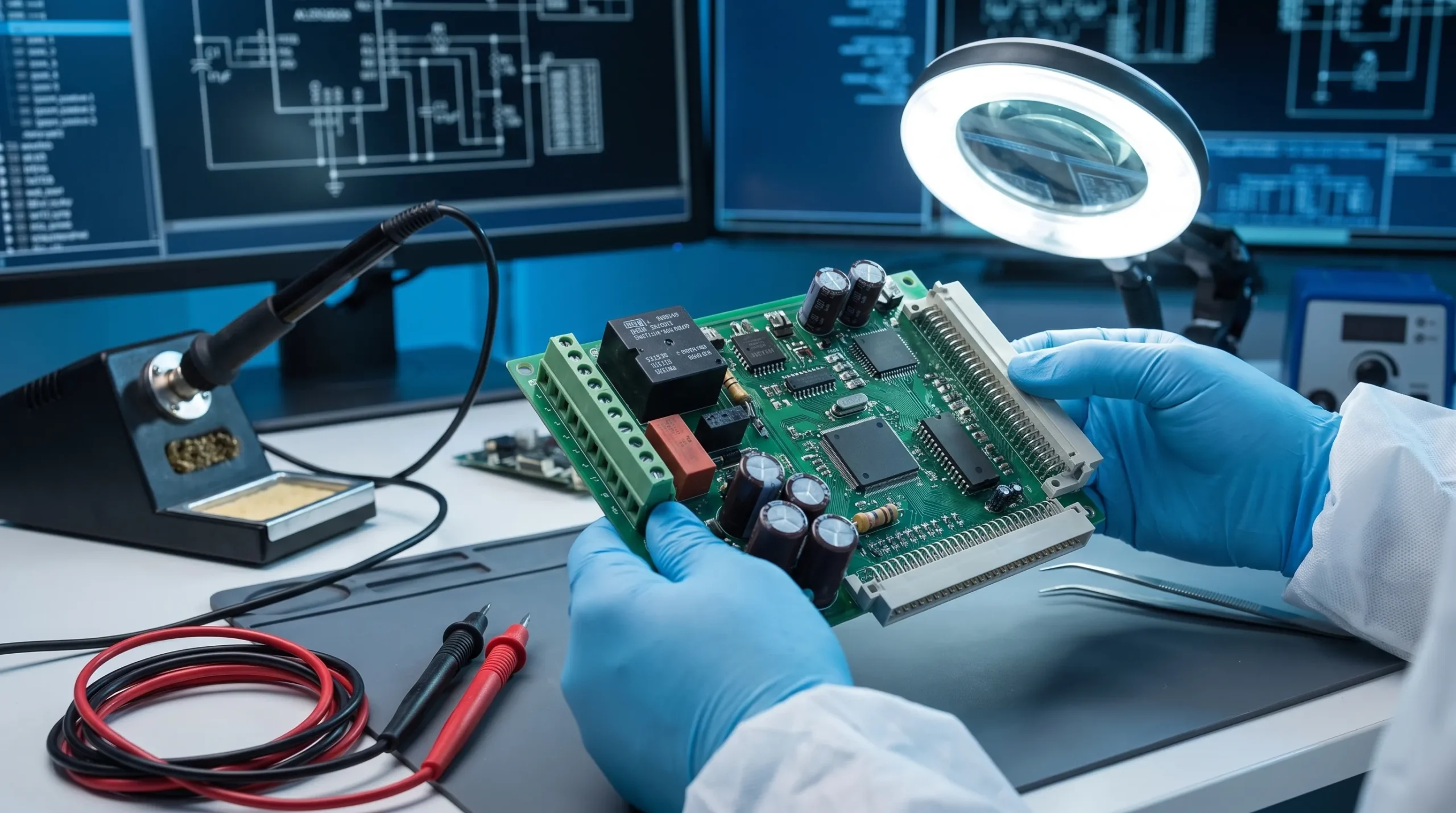
For many product teams, progress in circuit board design is associated with smaller packages, denser layouts and higher levels of surface mount automation. That is often justified. Modern SMT technology enables compact embedded systems, sensor-rich devices, wireless modules and sophisticated power control in a footprint that would have been impossible a generation ago.
Yet density is not always the primary design goal. In defence equipment, maritime systems, machine manufacturing, robotics, automotive products and industrial electronics, a connector pulled in the field or a power component exposed to thermal cycling can create more risk than a few extra square centimetres of PCB area. In those cases, a through hole circuit board, or a mixed board with selected through-hole components, can still be the more robust engineering choice.
The key is not to treat through-hole technology as automatically better. It is to understand where it reduces real product risk, where it introduces new constraints and how it fits into a complete system design.
What makes through-hole technology different
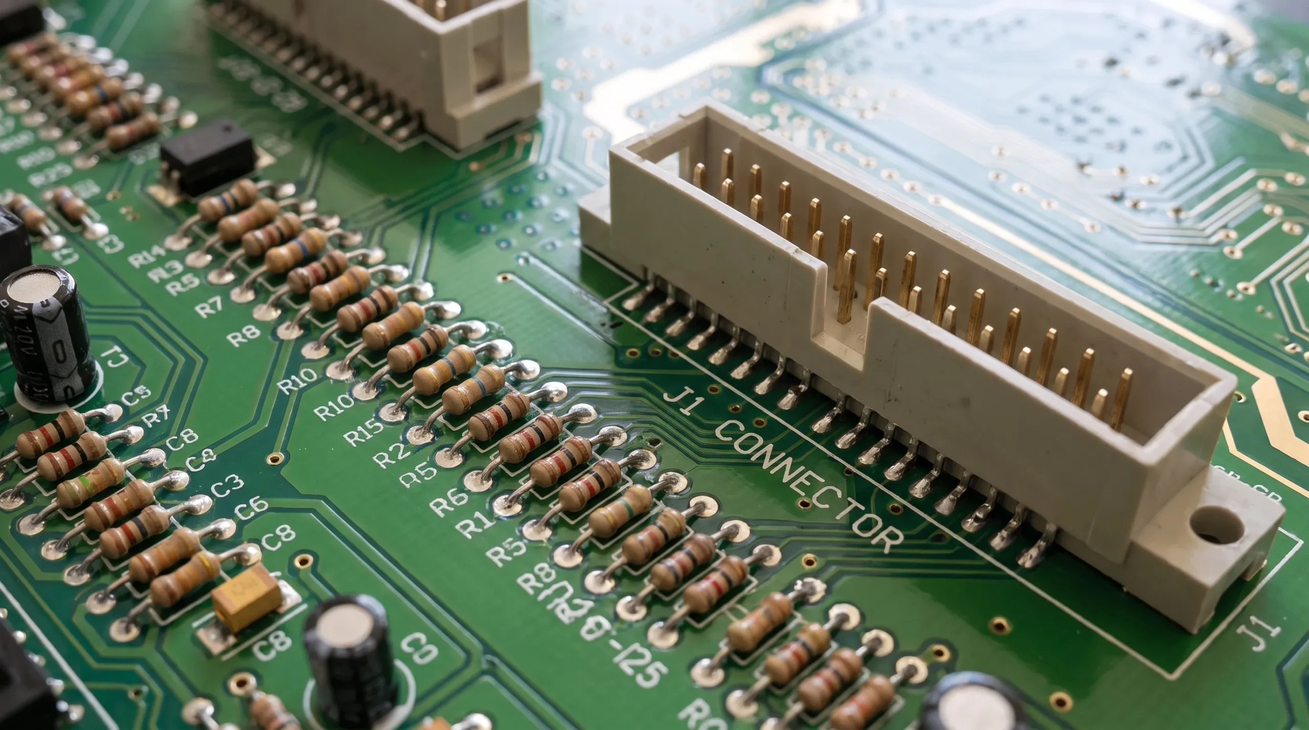
Through-hole components have leads that pass through drilled holes in the PCB and are soldered to plated pads, usually on the opposite side of the board. The lead, plated barrel and solder fillet together create a mechanical connection that can tolerate certain loads better than a surface mount joint.
Surface mount components sit on pads on the surface of the PCB. They are ideal for compact assemblies, automated placement and high component counts. For digital electronics, fine-pitch ICs, small passives and many analogue circuits, SMT is usually the default.
Through-hole still has a place because it changes the load path. A connector pin, terminal block lead, transformer pin or power device leg is supported through the thickness of the board rather than only on the copper pad surface. That can improve mechanical resilience when parts are subject to cable strain, repeated mating cycles, vibration or handling during service.
This distinction matters most when the PCB is part of a larger physical product. A board inside a sealed enclosure with fixed internal harnesses has different requirements from a board with user-accessible connectors on a machine, a maritime control box exposed to salt air or a motor drive mounted near vibration sources.
Through-hole versus SMT: the real trade-off
The choice between through-hole and SMT should rarely be ideological. It should follow the product requirements, operating environment, manufacturing route and lifecycle expectations.
| Design factor | Through-hole can help when | SMT is often better when | Engineering question to ask |
|---|---|---|---|
| Mechanical load | Connectors, relays, switches or heavy parts face strain, vibration or repeated handling | Components are small, protected and mechanically unloaded | Where will force enter the board during use or maintenance? |
| Density | Board area is available and robustness has priority | Product size, weight or routing density is critical | Is compactness a functional requirement or only a preference? |
| Thermal and current handling | Large leads, terminals or power parts need stronger physical connection and heat spreading | Heat can be managed through pads, vias, planes and packages | What is the real current path and thermal path? |
| Manufacturing efficiency | Volumes are moderate, components require selective soldering or serviceability matters | High-volume automated assembly is the priority | Which process will be stable at the intended production volume? |
| EMC and signal integrity | The part is low-frequency, power-related or mechanically critical | High-speed, RF or tightly controlled impedance paths are needed | Will the lead length or loop area create emissions or susceptibility issues? |
| Service and repair | Field replacement, inspection or ruggedisation is relevant | The product is sealed, compact and not repaired at board level | What maintenance model is expected over the product lifetime? |
A reliable product may use both technologies on the same PCB. Microcontrollers, sensors, memories, wireless modules and small passives may be SMT, while connectors, power terminals, large capacitors, magnetics and safety-critical interface components may remain through-hole. The quality of the result depends on how deliberately those choices are made.
When a through-hole circuit board makes engineering sense
A through-hole circuit board is most defensible when the component is part of the product’s mechanical, electrical or service interface. In other words, the technology choice should map to a stress mechanism.
In machine manufacturing, for example, connectors and terminal blocks often carry cable loads from sensors, actuators, motor drives and safety circuits. Even with good enclosure design and strain relief, installation and maintenance can put force into the connection area. Through-hole terminals can provide additional mechanical anchoring, especially when combined with mounting hardware, keep-out zones and sensible routing around the connector footprint.
In maritime and defence applications, boards may face vibration, shock, humidity, temperature cycling and long service lives. Through-hole parts are not a substitute for environmental design, but they can form part of a more robust architecture when used for high-stress interconnects, power entry, fusing, relays or large passive components.
In power electronics, through-hole components are still common where current levels, creepage and clearance, thermal rise or physical package size make SMT less attractive. Large electrolytic capacitors, inductors, transformers, bridge rectifiers, fuses and terminal blocks may all be better suited to through-hole mounting in the right context.
In serviceable professional products, through-hole can also support maintainability. A board that is expected to stay in operation for many years may benefit from components that can be inspected and replaced more easily, provided this is compatible with safety, warranty and compliance requirements.
For broader design context, ProMicro has also covered how circuit board design decisions shape long-term reliability, including operating conditions, layout choices and material decisions that should be considered before the component technology is finalised.
Reliability depends on the implementation details
Choosing through-hole technology does not make a board reliable by itself. Poor hole sizing, weak annular rings, excessive thermal mass, uncontrolled soldering or unsupported heavy components can still cause failures. The design and manufacturing details decide whether the theoretical reliability advantage becomes a real one.
| Design or process detail | Why it matters for reliability |
|---|---|
| Hole diameter and lead fit | Too tight can cause insertion damage or poor wetting, too loose can reduce solder joint consistency |
| Annular ring size | A larger pad gives more tolerance for drilling, registration and mechanical stress |
| Plated barrel quality | Barrel integrity affects electrical continuity, thermal cycling performance and long-term robustness |
| Component standoff | Correct spacing can improve cleaning, cooling and stress relief under the component body |
| Lead forming | Bent or preloaded leads can transfer stress into pads or component seals |
| Soldering process | Wave, selective and manual soldering each create different thermal profiles and quality risks |
| Copper balance and thermal relief | Large copper areas can drain heat and create inconsistent solder joints if not designed carefully |
| Cleaning and coating | Residues, flux entrapment and poor coating coverage can increase leakage, corrosion or field failures |
Through-hole joints are particularly sensitive to process discipline. A large connector with several ground pins tied directly into copper planes can be difficult to solder evenly. If the design does not account for thermal mass, some pins may show poor barrel fill while others are overheated. A heavy component without proper mechanical support can fatigue the solder joints even if the board passed initial functional testing.
Designers also need to consider the interaction with enclosure design. If an external connector is mounted through-hole but the enclosure cut-out is misaligned, every mating event can push force into the PCB. If a large capacitor is not supported against vibration, its leads may become fatigue points. The PCB is only one part of the mechanical system.
Good through-hole design therefore requires collaboration between electronics, mechanical design, manufacturing engineering and the assembly partner. Workmanship standards are useful, but they cannot compensate for a footprint or assembly concept that creates avoidable stress.
EMC and signal integrity should not be overlooked
There is a common assumption that through-hole boards are more robust in every sense. Mechanically, they can be. Electrically, the answer depends on frequency, current loops, grounding and return paths.
Through-hole leads add length. That length adds inductance and can increase loop area. In low-frequency power sections this may be acceptable, but in switching power supplies, motor drives, fast digital interfaces or RF circuits it can become a source of emissions, ringing or susceptibility.
A through-hole connector carrying signals to the outside world also creates an EMC boundary. Cable shields, grounding strategy, filtering components, transient protection and enclosure bonding must be considered together. If the connector is rugged but the return path is poorly controlled, the board can still fail EMC testing or become sensitive to disturbances in the field.
For mixed boards, placement discipline is essential. High di/dt loops should remain compact. Decoupling should sit close to the relevant device pins. Sensitive analogue inputs should not be routed around noisy power terminals. Mechanical robustness and EMC performance must be designed together, not traded against each other at the end of the project.
This is why PCB technology selection should be part of the architecture discussion. ProMicro’s article on how PCB board design affects reliability and EMC explores this relationship in more detail, especially for products that need to perform consistently outside laboratory conditions.
Manufacturing implications of through-hole boards
Through-hole assembly can add process steps compared with a fully SMT assembly. Depending on the product, the board may require wave soldering, selective soldering, manual soldering, additional inspection or fixtures to protect SMT parts during secondary operations. None of this is a problem if it is planned early, but it can become expensive or inconsistent if discovered late.
In low to medium volumes, a controlled through-hole process may be perfectly acceptable. In higher volumes, the assembly concept should be reviewed carefully for repeatability, cost, inspection access and test coverage. A design that is easy to prototype manually may not be easy to build consistently at scale.
The practical manufacturing questions include:
- Can all through-hole parts be soldered with a stable, repeatable process?
- Are SMT parts protected from wave or selective soldering heat and solder contact?
- Is there enough spacing for solder nozzles, tooling, inspection and rework?
- Are heavy or tall components supported during handling, transport and operation?
- Can automated optical inspection, electrical test or functional test access the relevant features?
- Are component substitutions possible without redesigning the PCB or enclosure?
These questions should be answered before layout release, not after the first pilot build. Once the board is routed and the enclosure is fixed, manufacturability options narrow quickly.
The same principle applies to the wider supplier ecosystem. Professional companies often bring in specialist partners for work that is outside their core expertise, whether that is an EMC test house, a manufacturing engineering partner. The point is not to outsource responsibility, but to reduce avoidable risk by involving the right expertise at the right time.
For electronics, that means involving assembly and manufacturing knowledge while the design is still flexible. ProMicro’s guidance on PCB assembly and manufacturing for reliable electronics explains why early engineering decisions often have more impact on quality than the assembly step itself.

Where through-hole can create new risks
Through-hole technology is not the conservative choice in every situation. Used without a clear reason, it can increase board size, routing complexity and assembly cost. It can also make EMC performance harder to control in fast circuits.
In compact embedded systems, through-hole parts can block routing channels and force longer traces. That may increase layer count or compromise signal paths. In products with wireless communication, poorly placed through-hole metalwork can affect antenna performance, shielding behaviour or coupling between sections of the board.
Manual soldering is another risk area. It may be acceptable for prototypes and certain low-volume products, but uncontrolled manual soldering can introduce variation in heat exposure, flux residue, solder volume and joint appearance. For professional products, the manual process should still be specified, trained, inspected and documented.
Component availability also matters. Some through-hole packages remain widely available, especially for power and electromechanical parts. Others may have fewer modern alternatives than their SMT equivalents. For a product intended to remain in production for many years, the bill of materials should be assessed for lifecycle risk, second-source options and redesign impact.
Finally, through-hole can create a false sense of security. A connector with strong solder joints may still fail if the cable has no strain relief. A large capacitor may still fail early if ripple current and ambient temperature are underestimated. A rugged PCB can still be unreliable if requirements, derating, enclosure sealing or thermal paths are weak.
A practical decision framework
The best way to decide is to connect each through-hole choice to a specific requirement or risk. If no one can explain why a component needs to be through-hole, it may be there out of habit rather than engineering necessity.
Use through-hole deliberately when mechanical anchoring, serviceability, creepage, clearance, power connection or package availability justify the trade-off. Use SMT where density, automation, high-speed performance or compact routing matter more. Use a hybrid approach when different sections of the product face different stresses.
A useful design review can be built around four questions.
First, what will the board experience in real use? Include vibration, shock, installation handling, cable movement, humidity, temperature, contamination and maintenance actions. Lab conditions rarely represent the whole product life.
Second, where do loads enter the PCB? Connectors, switches, terminals and heavy components deserve special attention. The strongest solder joint is still not a replacement for proper mechanical design.
Third, how will the board be manufactured and tested at the intended volume? Prototype convenience should not dictate the production process. Selective soldering access, inspection coverage, test points, cleaning and coating all need to be designed in.
Fourth, what happens during the product lifecycle? Consider obsolescence, component alternatives, field service, documentation, compliance updates and production continuity. A reliable design is one that can be built, maintained and supported over time.
How ProMicro approaches through-hole design decisions
For ProMicro, the through-hole versus SMT decision is not just a PCB layout preference. It is part of the wider system engineering process. A board technology choice affects enclosure integration, embedded system architecture, power electronics, analogue interfaces, EMC behaviour, assembly strategy and long-term manufacturability.
That broader view is important for companies developing professional products. A prototype that works once on a bench is not the same as a product that can pass verification, survive real use and move towards volume manufacturing. Early choices around connectors, board stack-up, grounding, thermal design, component selection and test access can decide how difficult that journey becomes.
In practice, ProMicro looks beyond the visible requirement. If a customer asks for a through-hole connector, the engineering question is not only whether that connector fits the PCB. It is whether the connector is exposed to load, whether the enclosure supports it, whether EMC filtering is placed correctly, whether assembly can solder it consistently and whether the component remains suitable for the product’s lifecycle.
That type of review can prevent late redesigns. It also helps internal engineering teams when they need extra specialist capacity in embedded systems, power electronics, analogue electronics, PCB design, prototyping or manufacturing preparation.
Frequently asked questions
Is a through-hole circuit board always more reliable than an SMT board? No. Through-hole can improve mechanical robustness for certain components, but overall reliability depends on the full design, including layout, soldering process, enclosure, thermal management, EMC design and component selection.
When should through-hole components be used in a modern PCB? They are often useful for connectors, terminal blocks, relays, large capacitors, magnetics, fuses, power entry points and other components exposed to mechanical stress, higher current, heat or service requirements.
Can through-hole boards meet EMC requirements? Yes, but through-hole construction does not guarantee good EMC performance. Lead length, loop area, grounding, filtering, cable interfaces and return paths must be designed carefully, especially in switching, motor control and communication circuits.
Does through-hole assembly make volume manufacturing harder? It can add process steps such as wave soldering, selective soldering or manual soldering. These steps can be controlled, but they need early design-for-manufacturing review to avoid inconsistent quality or unnecessary cost.
Is a mixed SMT and through-hole board a good compromise? Often, yes. Many professional products use SMT for dense electronics and through-hole for mechanically stressed or power-related components. The important point is to define the reason for each technology choice.
Need to make the right PCB technology choice?
If your product must survive vibration, field service, electrical stress or demanding operating conditions, the choice between SMT, through-hole and a hybrid PCB should be made early in the development process.
ProMicro supports companies with embedded systems, power electronics, analogue electronics, PCB design, prototyping and preparation for volume manufacturing. If you need a technical partner who can assess reliability, manufacturability, EMC risk and lifecycle impact together, ProMicro can help you turn a robust concept into production-ready electronics.