
Power electronics often look successful in the lab long before they are ready for the field. A converter regulates at nominal load, a motor drive spins the actuator, a battery interface charges correctly, and the first PCB passes basic functional checks. The real test comes later, when the product is exposed to heat, load transients, long cables, mechanical constraints, production variation, electromagnetic disturbance and compliance testing.
That is why reliable power electronics design is not only about selecting the right topology or calculating efficiency. It is a system engineering challenge. Reliability, EMC and scalability are connected from the first architectural decisions through PCB layout, enclosure integration, firmware behaviour, validation and manufacturing preparation.
For OEMs, machine builders and high-tech product teams, this matters because late changes in power electronics are rarely small. A modified switching frequency may affect filters, thermal performance, control stability, firmware settings, component ratings, PCB layout and certification planning. A poor early decision can therefore create cost, delay and field risk.
The practical objective is clear: design the power stage as part of the full product, not as an isolated circuit.
Reliability starts with the real operating envelope
A power electronics design can only be reliable when the team understands the conditions in which it must operate. Many issues arise because the prototype was designed around nominal values, while the real product is exposed to worst-case combinations.
For example, a motor drive may need to handle stalled motors, regenerative energy, long cable runs, harsh transients and repeated thermal cycling. A DC-DC converter in an embedded system may operate inside a sealed enclosure with limited airflow, while sharing space with sensors, RF modules and analogue front ends. A charger or battery-powered system may see variable input sources, user errors and ageing cells.
The requirement set should therefore go beyond voltage, current and efficiency. It should capture the environment, duty cycle, installation context, user behaviour, service expectations and production target.
| Requirement area | Typical hidden risk | Design consequence |
|---|---|---|
| Input source | Brown-outs, surges, reverse polarity, load dumps or unstable supplies | Protection, filtering, hold-up strategy and safe start-up behaviour |
| Load profile | Peak currents, stalled motors, inrush, regeneration or pulsed loads | MOSFET selection, current sensing, thermal margin and fault handling |
| Thermal environment | Sealed enclosure, solar heating, poor airflow or nearby heat sources | Derating, heat spreading, enclosure design and temperature monitoring |
| EMC environment | Long cables, antennas, inductive loads, neighbouring electronics or metal structures | Layout strategy, grounding, shielding, filtering and cable management |
| Compliance route | EMC, RED, CE, safety or sector-specific requirements | Early design constraints, documentation and pre-compliance planning |
| Production scale | Component tolerances, test time, assembly variation and supplier changes | Design for manufacturing, test points, BOM control and lifecycle planning |
This is where experienced engineering teams separate the explicit requirements from the hidden ones. The explicit requirement may be a 48 V input and 500 W output. The hidden requirement may be that the unit sits next to a radio module, runs in a warm enclosure, must survive incorrect field wiring and will later need a cost-controlled PCBA test strategy.
Architecture decisions shape EMC and reliability
Before schematic details are finalised, the architecture already defines many of the risks. Topology, isolation strategy, switching frequency, grounding concept, measurement method and protection philosophy all influence reliability and EMC.
In power electronics, there is rarely one perfect architecture. Each option introduces trade-offs. A higher switching frequency may reduce magnetics size, but increase switching losses and radiated emissions. A compact layout may improve loop area, but make thermal spreading or isolation distances harder. A faster gate drive may improve efficiency, but increase ringing and common-mode noise. A more aggressive cost target may reduce margins and make production variation more visible.
The architecture phase should therefore include technical risk analysis, not only component selection. Useful questions include:
- Which energy paths carry high di/dt or high dv/dt currents?
- Where will fault energy go during overload, short circuit or regeneration?
- How will measurement accuracy be maintained near noisy switching nodes?
- Which functions must remain safe if firmware resets or a sensor fails?
- What parts of the design are most sensitive to layout, temperature or tolerance spread?
- How will the same design be tested, calibrated and maintained in production?
This early architecture work reduces the chance of discovering fundamental design conflicts during EMC testing, pilot builds or customer field trials.
For related background on why standard modules can become problematic in real installations, see ProMicro’s article on custom power electronic solutions.
Designing for thermal reliability
Thermal performance is one of the most common reasons why power electronics behave differently outside the lab. A prototype on an open bench may run acceptably, while the same design inside a compact enclosure becomes unstable, derates too early or ages faster than expected.
Thermal reliability is not solved by adding a heatsink at the end. It must be designed into the power path, PCB stack-up, component placement, enclosure and operating strategy.
Key design considerations include semiconductor conduction and switching losses, inductor and transformer losses, capacitor ripple current, connector heating, copper thickness, thermal vias, airflow assumptions and enclosure coupling. The impact of ageing should also be considered, particularly for components where lifetime depends strongly on temperature and ripple current.
A robust design uses realistic loss calculations and then validates them with measurement. Thermal cameras, thermocouples and logged operating data can reveal hotspots that are not obvious from a schematic. However, measurement must be performed under representative load conditions. A product intended for a machine, vehicle, maritime installation or defence application should not only be tested in a comfortable lab environment.
Firmware can also support thermal reliability. Soft-start, current limiting, thermal derating, controlled restart behaviour and fault logging can prevent a temporary abnormal condition from becoming permanent damage. In embedded systems, hardware and software decisions must therefore be made together.
EMC is created by current paths, not fixed by filters alone
Electromagnetic compatibility is often treated as a late-stage test topic, but in power electronics it is strongly determined by the layout and system architecture. Switching converters and motor drives create steep voltage and current transitions. If those transitions are not controlled, the product can disturb itself or other equipment.
The IEC describes electromagnetic compatibility as the ability of equipment to function satisfactorily in its electromagnetic environment without introducing intolerable electromagnetic disturbance to anything in that environment. For a practical introduction, ProMicro has also covered what EMC means for electronic products.
In power electronics, EMC issues are often caused by a combination of factors rather than a single component. High-frequency current loops, parasitic capacitance, poor return paths, long cables, inadequate shielding, uncontrolled gate drive behaviour and insufficient separation between noisy and sensitive circuits can all contribute.
Filters are important, but they should not be the only strategy. If the PCB layout creates a large antenna, a filter may only reduce the symptom. If the enclosure has poor bonding, a cable shield may be ineffective. If analogue sensing is routed through a noisy ground path, software filtering will not solve the underlying disturbance.
| EMC challenge | Typical root cause | Early design action |
|---|---|---|
| Conducted emissions | Switching ripple, common-mode currents or inadequate input filtering | Define filter placement, return paths and impedance targets early |
| Radiated emissions | Large switching loops, fast edges, cables acting as antennas | Minimise loop area, control gate drive, manage cable exits and shielding |
| Immunity failures | Poor grounding, weak protection or sensitive resets | Add robust protection, watchdog strategy, filtering and layout separation |
| Sensor disturbance | Shared return paths or coupling from power nodes | Use careful partitioning, Kelvin sensing, differential measurement and analogue filtering |
| Enclosure interaction | Unplanned shield currents or poor bonding | Co-design PCB, cables, connectors and enclosure from the start |
Designing with EMC in mind does not guarantee a certification result, because final compliance depends on the full product, test configuration and applicable standards. It does, however, reduce the likelihood of late redesigns and improves the quality of the first compliance attempt.
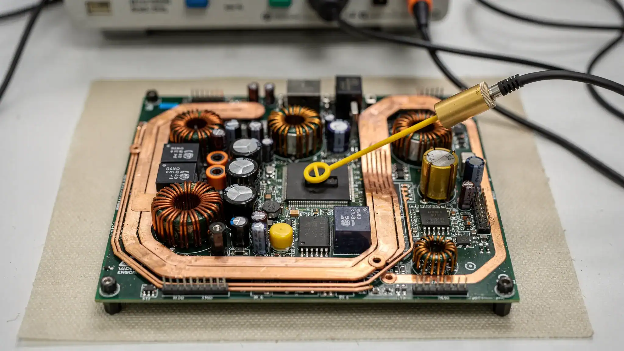
PCB layout is a functional part of the power stage
In low-speed circuits, layout mistakes may sometimes be corrected with minor changes. In power electronics, the PCB layout is part of the circuit. Parasitic inductance, capacitance, copper resistance and thermal paths directly influence switching behaviour, losses, noise and reliability.
A good PCBA design controls the critical current loops first. The input capacitor, switching device, diode or synchronous rectifier, inductor and return path must be arranged so that high-frequency energy stays local. Gate drive loops should be short and predictable. Current measurement should avoid noisy return paths. Sensitive analogue and digital signals should be kept away from switching nodes and power magnetics.
Power integrity and signal integrity are also connected. A microcontroller reset caused by a switching transient may look like a firmware issue, while the root cause is a layout or grounding problem. A sensor offset may appear to be calibration drift, while the actual problem is common-mode noise from the power stage.
For higher voltage or safety-relevant designs, creepage, clearance and insulation coordination must be considered alongside layout density. Thermal copper must be balanced with solderability and manufacturability. Test points must be accessible without compromising EMC. Connectors should be selected not only for current rating, but also for installation, vibration, serviceability and field wiring behaviour.
A useful rule is to treat the PCB review as a system review. The question is not only whether the schematic is connected correctly. The question is whether the physical implementation supports stable, safe and repeatable behaviour.
Protection and diagnostics reduce field risk
Power electronics must handle abnormal conditions gracefully. In many professional products, the power stage is connected to motors, batteries, solenoids, pumps, sensors, cable harnesses or external supplies. These interfaces create risk.
Protection should be designed as a layered strategy. Hardware protection can respond quickly to dangerous energy levels. Firmware can provide context, controlled restart, derating and fault logging. System-level design can ensure that a fault does not propagate into unsafe behaviour elsewhere in the product.
Common protection and diagnostic functions include overcurrent detection, overvoltage protection, undervoltage lockout, reverse polarity protection, thermal monitoring, short-circuit response, watchdogs, safe-state outputs and event logging. The right combination depends on the product, application environment and required safety concept.
Diagnostics are especially valuable when products move from prototypes to field deployment. If a product fails without recorded context, the engineering team may struggle to distinguish between installation error, component weakness, firmware behaviour, thermal overload or EMC disturbance. Capturing useful fault information can reduce investigation time and support future product improvements.
Scaling means more than producing more boards
Scale is often misunderstood as a manufacturing question that starts after engineering. In reality, scalability is designed from the beginning.
A power electronics prototype can be successful with hand-selected components, manual tuning, flexible lab wiring and direct engineering support. A production product cannot rely on those conditions. It must tolerate component variation, be assembled repeatedly, be tested efficiently and remain maintainable during its lifecycle.
Design for scale includes BOM strategy, component availability, second-source options where appropriate, test coverage, programming method, calibration approach, production documentation, assembly tolerances and enclosure integration. It also includes the ability to diagnose failures during production without requiring senior engineers to inspect every unit.
| Development stage | Main risk if scale is ignored | Practical mitigation |
|---|---|---|
| Concept | Requirements are too narrow and miss field or compliance constraints | Define operating envelope, standards route and production assumptions |
| Prototype | Lab success depends on manual adjustments or ideal conditions | Test worst-case loads, temperatures, cables and supply conditions |
| Engineering validation | EMC, thermal or protection weaknesses appear late | Use pre-compliance scans, thermal validation and fault injection |
| Pilot build | Assembly variation causes inconsistent behaviour | Improve test points, tolerances, documentation and PCBA feedback loops |
| Volume manufacturing | Component shortages or test bottlenecks disrupt delivery | Manage lifecycle, alternatives, production test strategy and supplier communication |
For more detail on this transition, see ProMicro’s guidance on preparing a PCB design for prototyping and volume build.
Validation should follow the risk, not only the checklist
Testing is most effective when it is linked to the risks identified during architecture and design. A standard functional test confirms that the product works under selected conditions. A risk-based validation plan asks how the design behaves at the edges of its operating envelope.
For power electronics, useful validation often includes start-up and shutdown behaviour, load steps, overloads, short circuits, thermal soak, supply interruptions, cable variations, radiated and conducted pre-checks, sensor accuracy near switching activity, firmware recovery and production test repeatability.
The order of testing matters. Early bring-up should be controlled and instrumented, with current limits, thermal monitoring and clear stop criteria. As confidence grows, tests can move towards combined worst-case conditions. For example, high load, high ambient temperature and low input voltage may be more revealing than testing each factor separately.
A practical validation plan also defines what evidence will be kept. Measurement plots, thermal images, firmware logs, design calculations, test reports and design review records all help future maintenance, certification preparation and customer communication.
Engineering culture matters here. Teams that improve through feedback loops, mentoring and progressive responsibility tend to expose risks earlier. Outside electronics, the same principle can be seen in adaptive learning and continuous improvement, where progress depends on close feedback and sustainable development rather than one-off evaluation. In power electronics development, regular review cycles and measured learning serve a similar purpose: they help teams correct assumptions before those assumptions become expensive redesigns.
The role of enclosure, cables and mechanical integration
A power electronics board is rarely the whole product. Enclosure design, connectors, cable routing, grounding and mechanical constraints can all change electrical behaviour.
A metal enclosure may help shielding, but only if bonding and cable entry points are designed correctly. A plastic enclosure may reduce certain coupling paths, but provide little shielding and may create thermal challenges. Long cables to motors or sensors can increase emissions, susceptibility and transient stress. Connector placement can influence serviceability, ESD paths and assembly repeatability.
Mechanical integration also affects reliability through vibration, condensation, dust, salt exposure, cooling paths and user access. In maritime, defence, automotive, robotics and industrial environments, these factors are not secondary. They are part of the design problem.
This is why power electronics should be developed alongside system engineering and enclosure design. When the PCB, firmware, housing and cable concept are reviewed together, the team can avoid late discoveries such as a filter that no longer fits, a heatsink with no airflow, a shield that cannot be bonded or a test point that is inaccessible after assembly.
When to involve a specialist power electronics partner
Many companies have strong internal engineering teams, but power electronics can create capacity and expertise gaps. This is especially true when the product combines embedded software, sensors, connectivity, motor control, analogue measurement, safety considerations and compliance requirements.
Involving an external electronics design partner is particularly valuable when:
- The design must operate in a demanding electromagnetic or thermal environment.
- The product combines power electronics with embedded systems, wireless communication or sensitive analogue electronics.
- EMC, RED, CE or safety-related requirements may influence the architecture.
- The internal team needs additional capacity without losing ownership of the product vision.
- The prototype must become manufacturable, testable and maintainable for series production.
- The cost of a late redesign would be high due to tooling, certification, customer commitments or field liability.
The value of such a partner is not only schematic capture or PCB layout. It is the ability to think across disciplines and identify risks that may not be visible in the initial assignment.
Frequently asked questions
What is the biggest reliability risk in power electronics design? The biggest risk is designing around nominal conditions and discovering too late that the product behaves differently under heat, transients, load peaks, long cables or production variation. A clear operating envelope and early risk analysis reduce this risk.
How early should EMC be considered in a power electronics project? EMC should be considered during architecture, before the PCB layout is started. Switching topology, grounding, cable routing, enclosure concept, filter placement and gate drive behaviour all influence EMC performance.
Can EMC problems be solved after the prototype is built? Some EMC issues can be improved with filtering, shielding or firmware changes, but many root causes are created by layout and system architecture. Late fixes are often larger, more expensive and less predictable than designing with EMC in mind from the start.
What makes a power electronics design scalable for manufacturing? A scalable design has controlled tolerances, available components, accessible test points, clear production documentation, a practical PCBA test strategy and margins that do not depend on hand-tuning or ideal lab conditions.
Why combine power electronics, embedded systems and enclosure design in one development process? These disciplines influence each other. Firmware affects protection and diagnostics, PCB layout affects EMC and thermal behaviour, and the enclosure affects cooling, shielding and serviceability. Integrated development reduces hidden conflicts.
Develop power electronics with reliability, EMC and scale in mind
Power electronics development is most successful when reliability, EMC and manufacturability are treated as design inputs rather than late-stage checks. That requires a structured process, strong technical judgement and collaboration across hardware, firmware, analogue electronics, PCB design, enclosure design and manufacturing preparation.
ProMicro supports companies from concept to volume-ready electronics, with expertise in embedded systems, power electronics, analogue electronics, PCB design, rapid prototyping, system engineering and lifecycle thinking. The goal is not only to make a circuit work, but to create a robust electronic product that can perform in real conditions and be prepared for long-term use.
If your team is developing a high-value product, machine, connected device or embedded platform where power electronics reliability matters, contact ProMicro to discuss the technical risks, development route and next steps.