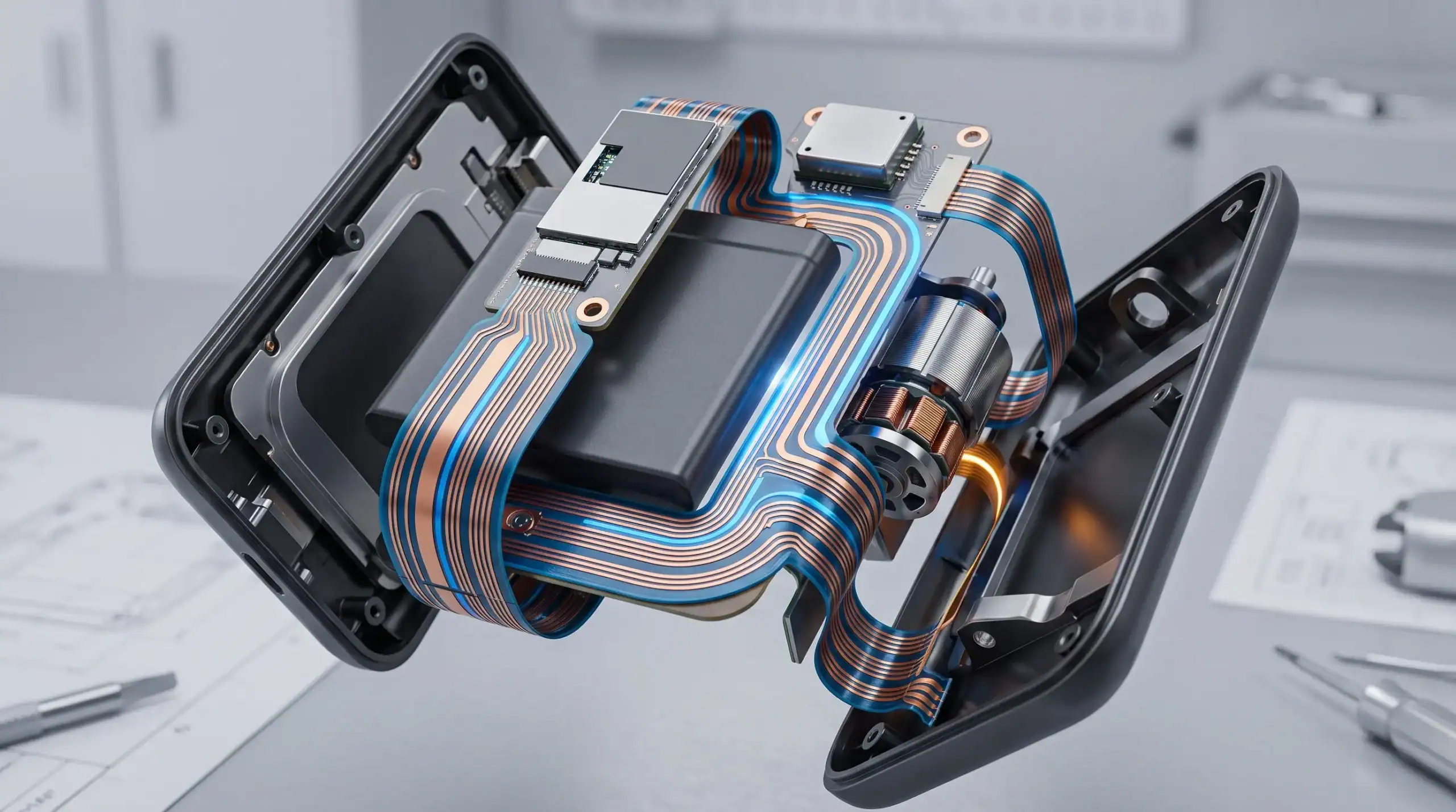
For compact electronic products, flex PCBs are rarely a simple packaging trick. They can remove connectors, fold circuitry around mechanical features and help fit sensors, displays, batteries or antennas into places where a rigid board cannot go. In high-tech equipment, robotics, automotive modules, maritime electronics and defence products, that can make the difference between a feasible product architecture and a housing that simply has no room left.
The engineering challenge is that every millimetre saved introduces another decision somewhere else. Bend performance, stack-up, EMC behaviour, thermal paths, assembly yield, test access and lifecycle support all become part of the same design conversation. A flex PCB should therefore be treated as an electromechanical subsystem, not as a thin version of a normal PCB.
If your team is still evaluating whether a flexible or rigid-flex architecture is justified, it is useful to first clarify when flexible PCBs make sense in product design. This article focuses on the next question: what trade-offs matter once a compact product starts to depend on flex technology?
Why compact products use flex PCBs
Flex PCBs are attractive because they allow electronics to follow the product shape. Instead of linking several rigid boards with wires, flat cables or board-to-board connectors, a flex or rigid-flex construction can create a controlled interconnect between functional areas.
That can bring clear benefits in space-constrained products. It may reduce assembly steps, improve repeatability, make the internal layout cleaner and remove potential connector failure points. It also gives mechanical designers more freedom to place electronics around batteries, motors, optics, antennas, actuators or enclosure ribs.
In professional products, the value is not only smaller size. A well-designed flex PCB can contribute to vibration resistance, sealing strategy, service life and manufacturability. A poorly designed one can do the opposite. The compact form factor may look successful in the prototype, then create field failures when repeated bending, temperature cycling, EMC exposure or production handling starts to reveal weaknesses.
Trade-off 1: space saving versus architectural complexity
The first trade-off is usually the most visible one. Flex PCBs save space by allowing a 3D layout, but they also make the system architecture more dependent on mechanical constraints. The position of every bend, stiffener, connector, component group and mounting point matters.
On a rigid PCB, late changes can sometimes be absorbed by rerouting or adjusting the outline. In a compact flex design, the electrical and mechanical layouts are tightly coupled. A small enclosure change can shift a bend line, increase strain in a copper track or make test pads inaccessible after folding. A component that fits electrically may become unsuitable if it sits too close to a dynamic section or creates a local stress concentration.
This is why flex PCB decisions should be made at system level. The development team needs to understand how the product will be assembled, opened, serviced, exposed to vibration and handled during production. That includes hidden requirements, such as the way a technician pulls a module out of a housing or how a cable-like flex tail moves when a robotic axis accelerates.
Trade-off 2: bendability versus mechanical lifetime
Flex PCBs can bend, but they do not all tolerate the same kind of bending. A static bend that is folded once during assembly is very different from a dynamic bend that moves thousands or millions of times in operation. The copper type, thickness, track direction, coverlay, adhesive system, bend radius and layer count all influence lifetime.
The common mistake is to treat minimum bend radius as a packaging target. In practice, a less aggressive bend often gives a more robust product. Tighter bends increase mechanical stress, especially at the outer copper layers and near transitions between flexible and rigid sections. Tracks crossing the bend perpendicular to the fold, abrupt width changes and vias in bend areas can all increase fatigue risk.
For deeper reliability guidance, ProMicro has a dedicated article on reliable flexible circuit board design, including bend radius, strain management and transition areas.
| Bend situation | Main benefit | Main risk | Design response |
|---|---|---|---|
| One-time assembly fold | Very compact packaging | Damage during assembly or rework | Define controlled fold areas, tooling and handling instructions |
| Occasional service movement | Easier maintenance access | Fatigue after repeated opening | Add strain relief, avoid copper concentration and validate service cycles |
| Continuous dynamic movement | Enables moving sensors or actuators | Copper fatigue and intermittent faults | Use suitable copper, generous radius, validated motion profile and life testing |
| Rigid-flex transition | Cleaner integration between board sections | Stress at the rigid-to-flex boundary | Use proper transition design, keep components away and avoid vias near the edge |
Trade-off 3: thin construction versus power and thermal performance
Flex PCBs are thin and lightweight, but compact power design still needs copper area, voltage spacing and thermal paths. This matters in motor drives, battery-powered equipment, robotics, automotive control units and sensor systems with local power conversion.
A thin flex layer may be excellent for signal routing but less suitable for high current unless track width, copper thickness and temperature rise are carefully managed. Heat has fewer places to go when the product enclosure is sealed, densely packed or made from low-conductivity materials. The design may need rigid sections, thicker copper, local heat spreaders, thermal vias in rigid areas or mechanical contact to the enclosure.
Voltage and safety spacing can also become difficult in compact flex layouts. Creepage and clearance rules do not disappear because the board bends. A folded construction can bring conductive areas closer together in 3D than they appear in the flat CAD view. For products designed with CE, EMC or safety requirements in mind, this needs to be reviewed before prototype layout is frozen.
The practical question is not whether flex can carry power. It can, within the right design envelope. The question is whether the required current, temperature rise, insulation system and product lifetime still make sense once the board is folded into the real housing.
Trade-off 4: component density versus assembly robustness
Compact products often tempt teams to place components wherever there is free copper. Flex PCBs make this tempting because the circuit appears to occupy very little volume before it is folded. Assembly reality is less forgiving.
Most components should sit on rigid or stiffened areas, not on active bend zones. Stiffeners can improve solder joint reliability and pick-and-place handling, but they add thickness, material interfaces and local rigidity. That may be exactly what the product needs, or it may create a stress riser if placed too close to a moving section.
Fine-pitch components, connectors, shielding cans and larger packages need careful review. A layout that is electrically correct may still be difficult to fabricate, panelise, assemble, inspect or rework. Adhesive squeeze-out, coverlay registration, solder mask choice, impedance control and fiducial placement can all influence quality.
This is where early supplier input matters. Fabrication and assembly are not afterthoughts in a flex design. Choices around materials, panel format, coverlay openings, stiffeners and inspection access affect product quality just as much as the schematic does. For a broader view of these production-related decisions, see ProMicro’s guide to PCB fab and assembly choices that affect product quality.
Trade-off 5: 3D routing freedom versus EMC and signal integrity
A compact flex PCB can place signals exactly where the product needs them, but the return path must follow. This is a major concern when flex circuits carry fast digital signals, sensitive analogue measurements, wireless interfaces or switching power waveforms.
In a rigid multilayer PCB, designers can often rely on stable reference planes. In a flex or rigid-flex design, the reference geometry may change along the interconnect. A folded flex can create loop areas, coupling paths and unintended antenna structures. Nearby motors, metal housings, batteries, displays and cable exits can also influence emissions and immunity.
Adding a ground plane, shield layer or controlled-impedance construction can improve EMC and signal integrity, but it may increase stiffness and reduce bend life. More layers can make routing cleaner but also make the flex less flexible. Shielding may solve one problem while creating another if it changes the mechanical behaviour or termination strategy.
For embedded products, EMC is rarely solved by one layout feature. It depends on partitioning, grounding, power architecture, filtering, enclosure design and cable strategy. Flex PCBs should be reviewed in that full context, especially if the product includes motor drives, wireless communication, sensors or analogue front ends.
Trade-off 6: integration versus test, repair and lifecycle support
Replacing several connectors and cables with one integrated flex assembly can improve repeatability and reduce assembly time. It can also make the product harder to test, repair or update if those needs are not designed in.
A compact folded assembly may hide test pads after the first assembly step. Boundary scan access, programming headers, calibration points and production test fixtures should be considered early. If a board must be folded before functional test, the test strategy may need dedicated contact areas or a temporary flat-state test process.
Repairability is another trade-off. A connectorised design may be bulkier but allows module replacement. An integrated rigid-flex assembly may be more robust in use, but a local fault can require replacement of a larger and more expensive assembly. For high-value professional equipment, the right answer depends on service model, warranty strategy, production volume and field environment.
Lifecycle support also includes documentation, traceability and component management. Long-lifecycle products need controlled BOM data, PCB revisions, firmware versions, test results and field feedback. In organisations where product and operational records span engineering, manufacturing and service teams, broader data lifecycle management can support the governance of that information beyond the PCB design environment.
Key design trade-offs at a glance
The table below summarises common flex PCB decisions in compact products. It is not a substitute for detailed engineering review, but it helps teams identify where early choices create downstream consequences.
| Design choice | What it can improve | What it can compromise | Review before committing |
|---|---|---|---|
| Replace cable harness with flex | Space, repeatability and assembly time | Repairability and routing freedom | Service model, test access and bend profile |
| Use rigid-flex instead of separate boards | Integration and vibration robustness | Fabrication cost and supplier complexity | Stack-up, panelisation and volume strategy |
| Add shield or ground layers | EMC and signal integrity | Flexibility and thickness | Bend radius, termination and return paths |
| Place components on stiffened flex | Packaging density | Local stress and assembly limits | Stiffener position, solder joints and inspection |
| Route power through flex | Compact power distribution | Temperature rise and voltage spacing | Copper weight, thermal path and safety margins |
| Minimise connectors | Reliability and sealing potential | Debugging, replacement and modularity | Production test, field service and lifecycle cost |
How to reduce risk before prototype build
The best time to reduce flex PCB risk is before the first prototype is laid out. At that stage, the team still has freedom to change the enclosure, split the electronics differently, move a connector, increase a radius or separate a high-current path from a dynamic section.
A practical flex PCB review should cover:
- The real motion profile, including assembly, servicing, vibration and transport loads.
- The flat and folded geometry, including clearance to metal parts, batteries, fasteners and enclosure ribs.
- The stack-up, copper type, layer count, shielding strategy and impedance requirements.
- The thermal path for power components, current-carrying tracks and local regulators.
- The EMC strategy, including return paths, filtering, cable exits and enclosure interaction.
- The manufacturing route, including panelisation, stiffeners, coverlay openings, assembly sequence and inspection access.
- The test strategy, including programming, calibration, production test and field diagnostics.
This type of review is especially valuable when the product combines embedded software, sensors, analogue electronics, wireless connectivity and power electronics in a compact mechanical package. The risks are often not isolated to the flex PCB itself. They appear at the interfaces between disciplines.
When flex PCBs may not be the right answer
Flex PCBs are powerful, but they are not automatically the best choice for every compact product. A conventional rigid PCB with a carefully chosen connector or cable may be more appropriate when the mechanical shape is still uncertain, production volumes are very low or service replacement is more important than internal volume reduction.
They may also be a poor fit if high current dominates the design, if the flex would need to bend sharply around unsuitable geometry or if the product will be exposed to uncontrolled handling without adequate strain relief. In some cases, the right decision is to redesign the mechanical architecture rather than force a flex circuit into an unrealistic path.
A good engineering partner should be willing to challenge the assumption that flex is needed. The goal is not to use the most advanced PCB construction. The goal is to create electronics that fit the product, pass through development with fewer avoidable risks and remain manufacturable over the intended lifecycle.
How ProMicro approaches flex PCB trade-offs
ProMicro looks at flex PCBs as part of the complete electronic product, not as an isolated layout task. In compact products, the PCB architecture affects embedded system behaviour, analogue performance, power integrity, EMC, enclosure design, assembly and long-term maintainability.
That is why early collaboration matters. By connecting system engineering, embedded development, power electronics, analogue design, PCB layout, prototyping and manufacturing preparation, ProMicro helps product teams expose design risks before they become expensive late-stage changes.
For engineering managers, CTOs and product development teams, this approach is especially useful when internal capacity is limited or when a product combines multiple technical domains. A flex PCB may solve a packaging problem, but only if it is designed around the real operating environment, compliance expectations and production route.
Frequently asked questions
Are flex PCBs reliable enough for professional products? Yes, if the stack-up, bend areas, materials, strain relief and operating conditions are designed correctly. Reliability problems usually come from treating a flex PCB like a normal rigid PCB or from discovering mechanical constraints too late.
What is the difference between flex and rigid-flex PCB design? A flex PCB is a flexible circuit that may connect to other boards or components. A rigid-flex PCB combines rigid board sections and flexible interconnects in one integrated construction. Rigid-flex can improve packaging and robustness, but it normally requires more careful stack-up, fabrication and assembly planning.
Can flex PCBs carry power as well as signals? They can carry power within suitable design limits. Current level, copper thickness, track width, temperature rise, bend behaviour and safety spacing all need review. In compact products, high-current areas may be better placed on rigid sections or supported by dedicated thermal design.
Do flex PCBs help with EMC? They can help by shortening interconnects and making routing more controlled, but they can also create EMC issues if return paths, shielding and folded geometry are not considered. EMC performance depends on the whole system, including grounding, filtering, enclosure design and cable strategy.
When should flex PCB decisions be made in the development process? They should be considered during architecture and mechanical concept development, not after the enclosure is nearly finished. Early decisions around bend radius, board partitioning, service access and production test can prevent costly redesigns.
Need support with a compact electronics design?
If your product depends on compact packaging, reliable embedded electronics, power electronics, analogue performance or manufacturing readiness, ProMicro can help assess the right PCB architecture early in the development process.
From concept and prototyping to production preparation, ProMicro supports technical teams with electronics design that is built around real-world use, compliance awareness and long-term reliability. Contact ProMicro to discuss how flex PCBs, rigid-flex layouts or alternative architectures could fit your next product development programme.