
A PCB that passes prototype testing is not automatically ready for volume manufacturing. In professional electronics, reliability depends on much more than a clean schematic and a working first build. Stack-up, component packages, solderability, test access, thermal behaviour, cable interfaces, enclosure constraints, documentation quality and lifecycle availability all influence whether a product can be built repeatedly with stable quality.
That is why a design for manufacturing PCB checklist should be used before layout release, not only when files are sent to a PCB fabricator or assembly partner. It gives engineering managers, technical directors, product owners and manufacturing stakeholders a shared way to identify risks while changes are still affordable.
For high-tech equipment, machine control, robotics, maritime systems, automotive electronics, defence applications and connected products, this checklist should sit between engineering intent and production reality. The goal is not only to make the PCB manufacturable. The goal is to make the complete electronic product reliable, testable, compliant-minded and scalable.
What design for manufacturing means for PCB volume builds
Design for manufacturing, often shortened to DFM, is the practice of designing a product so it can be manufactured consistently, economically and with controlled risk. For PCBs, this includes fabrication, assembly, inspection, testing, rework, environmental robustness and long-term supply.
A narrow DFM review checks track widths, hole sizes, solder mask clearances and component placement. Those checks are useful, but they are not enough for complex electronics. A stronger review also asks whether the PCB can survive its real operating environment, whether it can be tested efficiently, whether components will remain available, whether EMC risks are manageable and whether the design leaves enough margin for normal production variation.
For a broader process view, ProMicro has also explained how to prepare a PCB design for prototyping and volume build. This article takes a more checklist-driven angle, focused on the practical questions that should be answered before a design is released for reliable volume builds.
DFM PCB checklist at a glance
Use this overview as a gate review before approving a PCB for pilot or volume production. Each row should result in a clear engineering decision, not just a verbal confirmation.
| Review area | Critical question | Output before release |
|---|---|---|
| Product context | Does the PCB reflect the real operating environment and use case? | Approved requirements, environmental assumptions and compliance targets |
| System architecture | Are power, analogue, digital, sensing, motor drive and communication functions partitioned correctly? | Reviewed schematic, interface definition and risk register |
| Components | Are selected parts suitable for volume sourcing, assembly and lifecycle support? | Controlled BOM with approved alternates where appropriate |
| PCB fabrication | Can target fabricators build the stack-up, copper, vias and tolerances repeatably? | Fabrication drawing, stack-up specification and manufacturing constraints |
| Assembly | Can components be placed, soldered, inspected and reworked without avoidable risk? | Assembly drawing, placement review, panelisation approach and process notes |
| EMC and signal integrity | Are return paths, grounding, filtering and high current loops controlled by design? | Layout review evidence, pre-compliance plan and critical net review |
| Thermal and mechanical integration | Does the PCB work with the enclosure, mounting, airflow, heatsinking and service concept? | Mechanical interface review and thermal assumptions |
| Test and inspection | Can faults be detected efficiently during production? | Test points, programming access, functional test procedure and acceptance criteria |
| Documentation | Can a manufacturing partner build the product without hidden knowledge? | Complete release package with revision control and change process |
A checklist does not replace engineering judgement. It makes engineering judgement visible, repeatable and easier to discuss with manufacturing, compliance and product stakeholders.
Start with product context, not copper
Many DFM problems begin before the PCB layout starts. If the product context is vague, layout decisions become assumptions. Those assumptions may work in a lab prototype, then fail during EMC testing, environmental testing, field operation or production scaling.
A PCB for a motor-driven machine, for example, has different DFM risks from a battery-powered sensor node. A maritime product may face humidity, salt atmosphere and long service intervals. A defence or industrial control product may need robust connectors, controlled grounding and a clear approach to electromagnetic disturbance. A wireless IoT product may need antenna keep-outs, enclosure material decisions and regulatory planning from the start.
Before schematic freeze, confirm the following product-level inputs.
| Question | What to define | Why it matters for volume builds |
|---|---|---|
| Where will the product operate? | Temperature range, humidity, vibration, dust, salt, cleaning chemicals and installation conditions | Material choice, coating, connector selection and mechanical retention depend on the environment |
| What electrical interfaces leave the enclosure? | Power input, motor cables, sensor cables, antennas, communication ports and user-accessible connectors | External interfaces are common entry points for ESD, surge, conducted noise and mechanical stress |
| Which compliance routes are likely? | CE, EMC, RED for radio products, safety requirements and customer-specific standards | Late compliance findings can force layout, enclosure or component changes |
| How long must the product remain available? | Expected service life, repair strategy, component lifecycle and spare part policy | Long-lived products need stronger lifecycle planning than short-lived prototypes |
| How will production quality be verified? | ICT, flying probe, functional test, programming, calibration and traceability needs | Test access must be designed into the PCB, not added after layout completion |
This is also the moment to challenge hidden requirements. Does the product need to be maintainable in the field? Could users connect cables in the wrong order? Will a technician replace a module while power is present? Are there high energy circuits near sensitive analogue sections? These questions may not appear in the first specification, but they can determine whether the design is robust enough for real use.
Lock the architecture before the layout becomes expensive
A DFM review should not wait until the PCB is visually complete. By then, the most important choices may already be difficult to change. System architecture has a direct effect on manufacturability because it defines component count, board size, layer count, routing density, connector placement, thermal paths and test strategy.
For embedded systems that combine sensors, motor drives, wireless communication, power conversion and analogue measurement, the schematic review should include manufacturing consequences. A compact architecture may reduce board area, but it can also increase routing density, thermal coupling and inspection difficulty. A modular architecture may improve serviceability and test coverage, but it can introduce connector cost and signal integrity concerns.
Key architecture checks include the following.
| Architecture area | DFM check |
|---|---|
| Power input and protection | Confirm reverse polarity protection, inrush behaviour, fusing, surge tolerance, ESD protection and safe failure assumptions |
| Power rails | Review current budgets, voltage margins, sequencing, derating, ripple sensitivity and measurement access |
| Mixed-signal partitioning | Separate noisy and sensitive functions logically before placement begins, especially for analogue front ends and ADC references |
| Communications | Define termination, isolation, cable shielding, connector pinouts, ESD strategy and programming access |
| Firmware interfaces | Provide access for boot recovery, programming, debug, watchdog verification and production configuration |
| Safety-related boundaries | Confirm creepage, clearance, isolation and protective earth concepts against the applicable product context and standards |
The purpose is not to make the design larger or more conservative than necessary. The purpose is to avoid routing a PCB around an architecture that cannot be manufactured, tested or certified efficiently.
Select components for production, not only for function
A component that works electrically may still be a weak choice for volume builds. Availability, package style, moisture sensitivity, assembly process compatibility, thermal derating, inspection access and supplier stability all affect whether the design can move from prototype to production without disruption.
For critical parts, the BOM should document manufacturer part numbers, approved alternates where practical, lifecycle status and any special handling or programming requirements. This is especially important for microcontrollers, power semiconductors, sensors, RF modules, connectors, magnetics and precision analogue parts.
Component selection should also account for production variation. If a design depends on a narrow tolerance part, confirm whether the tolerance is genuinely required and whether the supply chain can support it. If a package has hidden pads, very fine pitch or special soldering requirements, confirm that the assembly partner can inspect and process it at the expected volume.
Use the following component checks before release.
| Component topic | What to verify | Risk if ignored |
|---|---|---|
| Lifecycle status | Active production, supplier notices and realistic availability | Redesign caused by end-of-life or allocation issues |
| Package suitability | Pick-and-place compatibility, solder joint inspectability and rework feasibility | Low yield, expensive inspection or difficult failure analysis |
| Derating | Voltage, current, temperature and power dissipation margins | Field failures under load, heat or production variation |
| Approved alternates | Electrical, mechanical, firmware and qualification impact of substitutes | Purchasing pressure leading to uncontrolled substitutions |
| Moisture and handling | MSL requirements and storage controls for sensitive packages | Solder defects during reflow |
| Connectors and cables | Mating cycles, retention, orientation, strain relief and service use | Intermittent faults and field reliability issues |
In high-value professional products, the cheapest part is not always the lowest-risk part. A slightly more suitable component can reduce certification risk, production downtime, rework and field service cost.
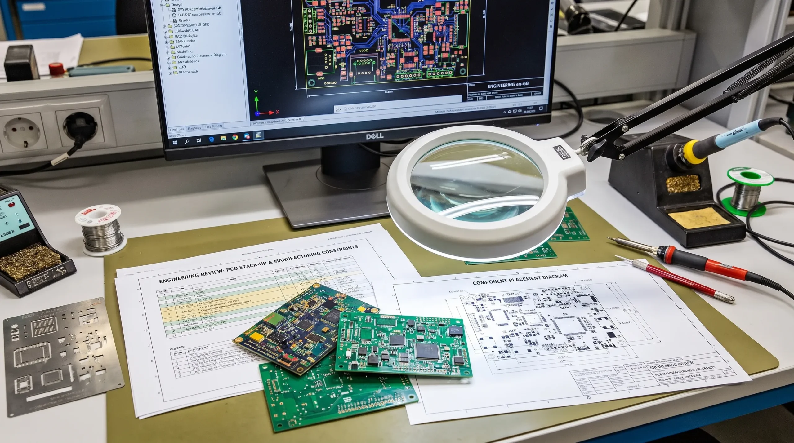
Confirm stack-up, materials and fabrication limits early
A reliable PCB is built within the stable capability of the chosen fabrication process. Designing to absolute minimum dimensions may be possible, but it can reduce yield margin and limit supplier options. For volume production, the question is not only whether a board can be fabricated once. The question is whether it can be fabricated repeatedly, inspected consistently and sourced over time.
ProMicro’s article on PCB board fabrication basics goes deeper into how fabrication choices influence reliability, EMC, thermal behaviour and supply. As a checklist item, the essential point is simple: fabrication constraints should be known before the layout is finalised.
| Fabrication topic | Confirm before release | Practical consequence |
|---|---|---|
| Layer count and stack-up | Target thickness, dielectric materials, copper distribution and reference planes | Affects routing, impedance, EMC, thermal paths and mechanical fit |
| Copper weight | Current carrying needs, thermal spreading and etching constraints | Heavy copper can influence spacing, soldering and fine feature capability |
| Minimum track and gap | Chosen rules sit comfortably within target supplier capability | Improves yield and avoids unnecessary dependence on advanced processes |
| Drilling and vias | Finished hole sizes, aspect ratio, via type and annular ring margin | Reduces plating reliability risks and fabrication rejects |
| Controlled impedance | Required nets, tolerance, reference planes and material data | Prevents late signal integrity issues on high-speed or RF interfaces |
| Surface finish | Compatibility with fine pitch, storage time, RoHS needs and assembly process | Influences solderability, shelf life and inspection quality |
| Panelisation | Rail width, tooling holes, fiducials, breakaway method and board edge stress | Affects assembly throughput and the risk of mechanical damage |
A practical rule is to design with manufacturing margin unless there is a strong technical reason not to. Margin in fabrication rules often becomes margin in yield, supplier flexibility and long-term product continuity.
Review layout for assembly, inspection and rework
Assembly problems are often visible in the layout long before a board reaches the production line. Tight component spacing, inconsistent orientation, poor fiducial placement, inaccessible test points, awkward connector positions and thermal imbalance can all increase the risk of defects or slow down production.
A PCB intended for volume build should be reviewed with the assembly process in mind. Surface mount components, through-hole parts, press-fit connectors, heatsinks, shields and mechanical fixings may require different process steps. If selective soldering, manual soldering, conformal coating, potting or post-assembly calibration is needed, the PCB layout should support those steps deliberately.
| Assembly topic | Checklist question | Why it matters |
|---|---|---|
| Component orientation | Are similar polarised components aligned consistently where possible? | Reduces placement errors and improves visual inspection |
| Fiducials and tooling | Are global and local fiducials, tooling holes and panel features agreed with the assembler? | Supports accurate pick-and-place and inspection |
| Spacing and keep-outs | Can nozzles, inspection systems and rework tools access critical areas? | Avoids low yield and difficult repairs |
| Thermal mass | Are large copper areas, heavy components and small passives balanced for reflow? | Reduces tombstoning, insufficient solder and thermal stress |
| Polarity and markings | Are reference designators, pin 1 marks and polarity indicators clear after assembly? | Improves inspection, service and failure analysis |
| Board edge features | Are connectors, tabs and depanelisation points positioned to avoid damage? | Prevents cracked joints and mechanical defects |
| Coating and cleaning | Are coating keep-outs, cleaning access and contamination risks defined? | Supports environmental protection without blocking connectors or test points |
DFM information should not live only in informal emails. If a decision affects assembly yield, inspection or rework, it belongs in controlled documentation.
Combine DFM with EMC, power integrity and analogue performance
A board can be easy to manufacture and still fail EMC testing. It can also pass EMC in one prototype configuration but become unreliable when cable routing, enclosure material or component substitutions change in production. For professional products, DFM and EMC should be considered together.
The most important layout decisions often involve current loops, return paths, grounding, shielding, filtering and the physical relationship between noisy and sensitive circuits. These are not cosmetic layout details. They determine whether switching converters, motor drives, radios, sensors and analogue front ends can coexist on the same PCB.
For products placed on the European market, the EMC Directive defines essential requirements for electromagnetic compatibility. Designing with EMC in mind reduces risk, but formal assessment and testing remain product-specific.
| Risk area | DFM and engineering check |
|---|---|
| Switch-mode converters | Keep high di/dt loops compact, provide solid return paths and control heat around power components |
| Motor drives | Review gate drive loops, current sensing, snubbers, connector placement and cable-related emissions |
| Analogue measurement | Protect reference nodes, minimise noise coupling and keep sensor inputs away from switching currents |
| Wireless functions | Preserve antenna keep-outs, ground reference needs and enclosure effects throughout mechanical design |
| External interfaces | Place ESD and filtering close to entry points and consider chassis bonding early |
| High-speed signals | Confirm impedance, length matching where needed, return paths and connector transitions |
For more detail on this combined view, see ProMicro’s guide to printed circuit board design for EMC and manufacturability. The key lesson for volume builds is that EMC fixes added late can create manufacturing issues, while manufacturing changes made late can disturb EMC behaviour.
Check thermal, mechanical and environmental integration
A PCB does not operate in isolation. It is mounted in an enclosure, connected to cables, exposed to users or technicians, and subjected to heat, vibration, contamination and maintenance conditions. A volume-ready DFM checklist must therefore include mechanical and environmental integration.
Thermal review should cover more than maximum component temperature in a simulation. It should consider airflow assumptions, enclosure material, heat transfer paths, copper spreading, mounting points, nearby heat sources, derating and the effect of dust or blocked ventilation. If the product is sealed, potted or conformally coated, heat dissipation and repairability may change significantly.
Mechanical review should confirm that the PCB is not stressed by mounting screws, connector insertion forces, cable pull, depanelisation tabs or enclosure tolerances. Heavy components may need additional retention. Board-to-board connectors need alignment tolerance. User-accessible connectors need mechanical support that does not rely only on solder joints.
Environmental protection also affects manufacturability. Conformal coating may improve robustness in humid or contaminated environments, but it requires keep-outs, process control and inspection criteria. Potting can protect against vibration or moisture, but it can complicate heat transfer, rework and failure analysis. These decisions should be made at product level, not as last-minute production additions.
Design for test before the first pilot build
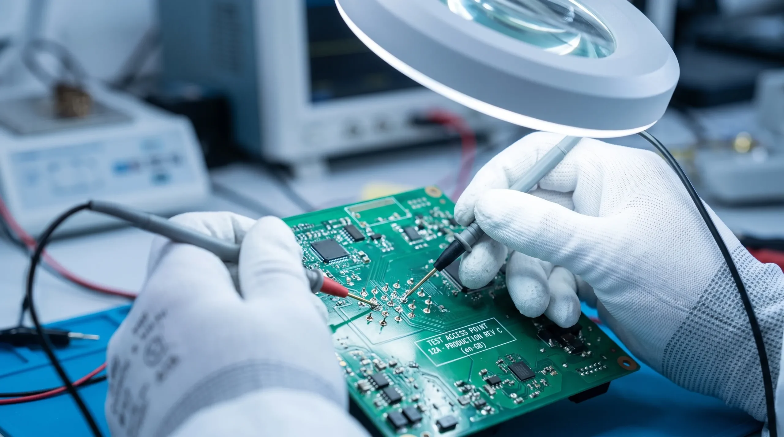
Testing is often treated as a production activity, but testability is a design property. If a PCB lacks access to critical rails, programming pins, communication interfaces or measurement points, production testing becomes slower, less reliable or more dependent on manual work.
A strong design for manufacturing PCB review should include design for test, often called DFT. The objective is not to test everything in the most expensive way. The objective is to detect likely faults efficiently, protect downstream assembly steps and create useful data for yield improvement.
| Test objective | PCB design provision | Value in volume production |
|---|---|---|
| Power-on safety | Accessible input current measurement, key rail test points and safe startup procedure | Detects shorts, wrong components and assembly defects before damage occurs |
| Programming | Reliable access to SWD, JTAG, UART, USB or other programming interfaces | Supports repeatable firmware loading and recovery |
| Functional test | Test modes, accessible connectors and defined loads or stimulus points | Verifies product behaviour without excessive manual probing |
| Calibration | Stable references, measurement access and calibration data storage | Enables controlled performance for sensors and analogue circuits |
| Traceability | Serial number, revision marking, label area or machine-readable code | Links test results to hardware revision and production history |
| Inspection | Clear reference designators, polarity marks and inspectable solder joints | Speeds up AOI, visual inspection and failure analysis |
Test limits should be based on engineering understanding, not arbitrary values copied from prototype measurements. Early pilot data can then be used to refine limits before volume release.
Build a complete documentation release pack
A PCB is not ready for volume manufacturing until the documentation is complete enough for someone outside the design team to build, inspect and test it. Missing or ambiguous documentation forces suppliers to make assumptions. Those assumptions can lead to inconsistent builds, uncontrolled substitutions and difficult root cause analysis.
At minimum, a release pack should include the controlled schematic, PCB fabrication data, assembly data, BOM, drawings, test procedure and revision history. Many organisations also include ODB++ or IPC-2581 data, pick-and-place files, approved vendor lists, programming files, coating drawings, panelisation data and packaging requirements.
| Release item | Why it matters |
|---|---|
| Fabrication data | Defines copper, drill, solder mask, silkscreen, finish, stack-up and tolerances |
| Assembly data | Defines placement, orientation, reference designators, special process steps and inspection needs |
| Controlled BOM | Prevents unintended substitutions and supports sourcing decisions |
| Approved alternates | Allows purchasing flexibility without uncontrolled engineering change |
| Test procedure | Gives production a repeatable way to verify build quality |
| Firmware and configuration files | Ensures hardware and software revisions remain aligned |
| Acceptance criteria | Clarifies what is acceptable, what requires rework and what requires engineering review |
| Change process | Controls deviations, ECOs and lessons learned from pilot builds |
Relevant industry standards from organisations such as IPC can help define acceptability, workmanship and design expectations. The applicable class and standard set should be chosen based on product risk, customer requirements and regulatory context.
Use pilot builds to prove the process, not only the design
A pilot build is not just a larger prototype. It is the first serious test of the manufacturing process, documentation, test strategy, supplier communication and design margin. Treat it as a learning stage with clear evidence requirements.
| Build stage | Main purpose | Evidence to collect |
|---|---|---|
| Engineering prototype | Prove core functionality and identify major design risks | Measurements, debug notes, early EMC checks and thermal observations |
| Design verification build | Use more representative layout, components, enclosure and firmware | Reliability findings, compliance pre-checks and design corrections |
| Pilot build | Exercise the intended production process and documentation | Yield data, assembly feedback, test coverage, rework causes and operator questions |
| Production release | Freeze a controlled baseline for repeatable builds | Approved files, ECO status, test limits, supplier approvals and release sign-off |
The most useful pilot build output is not a perfect first yield. It is a clear understanding of what failed, why it failed and whether the corrective action belongs in design, process, documentation, supplier selection or test coverage.
Common DFM mistakes that create volume-build risk
The same problems appear repeatedly when prototypes are pushed into production too quickly. They are rarely caused by a single poor layout decision. More often, they come from missing communication between product, electronics, mechanical, firmware, compliance and manufacturing stakeholders.
Common mistakes include releasing a layout before the target fabrication rules are known, choosing components without lifecycle review, leaving test access until after placement, treating the enclosure as separate from EMC behaviour, relying on hand assembly techniques that cannot scale, and allowing manufacturing notes to remain outside the controlled release package.
Another frequent issue is assuming that a lab prototype proves the complete product. In reality, lab prototypes often use different cables, power supplies, enclosures, firmware settings, assembly methods or component sources from the final product. Those differences can hide risks until certification, pilot build or field deployment.
The best time to reduce these risks is before schematic freeze and before placement freeze. The second-best time is before the first pilot build. After volume production has started, each correction affects stock, documentation, supplier communication, customer deliveries and sometimes compliance evidence.
Frequently asked questions
What is a design for manufacturing PCB checklist? A design for manufacturing PCB checklist is a structured review used to confirm that a PCB can be fabricated, assembled, inspected, tested and supported in production. It covers layout rules, component choices, documentation, test access, EMC considerations, thermal behaviour and manufacturing process constraints.
When should DFM be reviewed in a PCB project? DFM should be reviewed at several points: during requirements definition, before schematic freeze, before placement freeze, before layout release and after the pilot build. Waiting until files are ready for fabrication is too late for many architectural and testability improvements.
Is DFM only the responsibility of the PCB layout engineer? No. PCB layout is important, but DFM also involves system engineering, component engineering, embedded software, mechanical design, compliance planning, purchasing, manufacturing and test engineering. Reliable volume builds require decisions across all of these areas.
How is DFM different from DFT? DFM focuses on whether the PCB can be manufactured repeatably, while DFT focuses on whether faults can be detected efficiently during production. They overlap because test points, programming access, component placement and documentation all affect both manufacturability and production quality.
Can a prototype that works in the lab still fail in volume production? Yes. A lab prototype may not expose production variation, supplier substitutions, reflow effects, cable emissions, enclosure interactions, thermal stress, vibration or test coverage gaps. Volume readiness requires evidence from representative builds and controlled documentation.
Which standards should be considered for PCB volume builds? The relevant standards depend on the product, market and risk level. Many teams consider IPC workmanship and design standards, CE-related requirements, EMC requirements, RED for radio products and any sector-specific customer or safety standards. The design should be developed with these requirements in mind, while formal compliance remains product-specific.
Need support turning a PCB design into a reliable volume build?
If your product combines embedded systems, power electronics, analogue electronics, sensors, motor drives, wireless communication or demanding environmental requirements, DFM should be part of the development process from the start.
ProMicro supports companies from early product ideas through PCB design, prototyping and preparation for volume manufacturing, with attention to reliability, manufacturability, lifecycle risks and compliance-minded engineering. To discuss a design review or a complete development project, contact ProMicro’s electronics design specialists.