A PCB can meet its nominal copper-weight specification and still run too hot in service. In professional electronics, pcb board making affects the finished conductor thickness, etched trace geometry and plated connections that determine resistance. Current capacity then depends on how effectively the complete product removes the resulting heat.
For motor drives, power converters, robotic controllers and industrial equipment, this distinction matters. A prototype that operates on an open bench may behave differently inside a sealed enclosure, next to hot components or during repeated overloads. Specifying “2 oz copper” alone does not establish a safe operating current.
The engineering task is to connect fabrication requirements with electrical losses, allowable temperatures and evidence from representative testing. That starts with understanding which copper thickness is being specified and where the current actually flows.
How pcb board making determines finished copper thickness
Copper weight describes the mass of copper per unit area. It is commonly expressed in ounces per square foot and converted into a nominal thickness.
| Copper weight | Approximate nominal thickness | Engineering interpretation |
|---|---|---|
| 0.5 oz/ft² | 17 µm | A thickness designation, not a current rating |
| 1 oz/ft² | 35 µm | Must be related to finished conductor geometry |
| 2 oz/ft² | 70 µm | Offers lower resistance at the same finished width |
| 3 oz/ft² | 105 µm | Requires fabrication and layout capability checks |
These values are approximate conversions, not guaranteed minimum finished thicknesses. Procurement documents must distinguish starting foil from finished copper and define the acceptance requirements for each relevant layer.
The useful output of pcb board making is a controlled conductor cross-section, not simply an ounce rating. Two boards described as having the same copper weight can differ electrically if their finished track widths, plating requirements or acceptance criteria differ.
Outer layers: starting foil plus plating
In many plated-through-hole fabrication processes, outer-layer copper includes starting foil and additional deposited copper. A fabricator may begin with thinner foil and build towards the required finished thickness through plating.
The exact sequence depends on the process. Copper distribution can vary with panel position, feature density and plating conditions, so nominal deposited thickness should not be treated as a guaranteed local minimum everywhere.
Etching also affects the result. A finished track is not necessarily a perfect rectangle: undercut and sidewall shape change its effective cross-sectional area. The dimensions drawn in CAD therefore need to be reconciled with the fabricator’s finished-feature tolerances.
Surface finishes such as ENIG, immersion tin or OSP should not be credited as additional current-carrying copper.
Inner layers and via barrels need separate requirements
Conventional inner-layer conductors generally derive their thickness from the selected copper foil rather than the outer-layer plating process. Etching still determines their finished width and profile.
Via barrels are different again. Their conducting area depends on hole diameter and wall-plating thickness, not on the thickness of an adjacent copper plane. A thicker plane does not automatically produce a thicker or more reliable plated hole.
In pcb board making, track copper and barrel copper therefore need separate acceptance criteria. IPC-6012, Qualification and Performance Specification for Rigid Printed Boards, is a relevant specification framework, but the applicable revision, class and project-specific requirements must be agreed with the supplier.
For demanding products, drawings should make these distinctions explicit rather than relying on a single general note stating the board’s copper weight.
Current capacity is a thermal limit, not a copper-weight rating
Increasing conductor cross-section reduces resistance. It does not establish current capacity without a temperature limit and a defined operating environment.
A track reaches an operating temperature through the balance between electrical heating and heat removal. That balance changes with ambient temperature, nearby components, copper distribution, laminate construction, mounting and airflow. Internal and external tracks can behave differently, but there is no universal multiplier that captures every stack-up and installation.
IPC-2152, Standard for Determining Current Carrying Capacity in Printed Board Design, provides a recognised reference for assessing conductor temperature rise. Its information should be applied with attention to the board construction and thermal conditions, not treated as a universal current-rating table.
For pcb board making, this means the fabrication specification must support a thermal assessment based on the intended product environment.
Define the permitted conductor temperature using component limits, laminate requirements, insulation considerations and reliability objectives. A 20 °C temperature rise above a 25 °C ambient is a different operating condition from the same rise above a 70 °C ambient.
For pulsed or varying loads, RMS current helps assess resistive heating. Peak current, pulse duration and fault-clearing time also require assessment. In high-frequency power circuits, skin and proximity effects can make a DC-resistance-only calculation insufficient.
Calculate resistance before assigning an operating current
For a uniform rectangular copper track, a useful first-order calculation is:
R = ρL / (wt)
Here, ρ is copper resistivity, L is track length, w is finished width and t is finished thickness. At approximately 20 °C, copper resistivity is about 1.72 × 10⁻⁸ Ω·m.
Consider a 100 mm long track with a uniform 2 mm finished width carrying 10 A DC. The following calculation assumes ideal rectangular geometry and excludes pads, vias, connectors and current crowding.
| Finished copper thickness | Track resistance at 20 °C | Voltage drop at 10 A | Track dissipation at 10 A |
|---|---|---|---|
| 35 µm | 24.6 mΩ | 0.246 V | 2.46 W |
| 70 µm | 12.3 mΩ | 0.123 V | 1.23 W |
Doubling thickness halves resistance in this simplified case. It also halves dissipation at the same current because P = I²R.
These figures do not establish that either track can safely carry 10 A. They establish the heat that must be removed under the stated assumptions.
That calculation connects pcb board making tolerances directly to voltage drop and wasted power. If both finished width and thickness were 10% below the assumed values, cross-sectional area would be 81% of the original value and resistance would rise by about 23%. This is an illustrative sensitivity check, not a claim about standard fabrication tolerances.
Copper resistance also increases with temperature. Using a temperature coefficient of approximately 0.0039/°C, resistance at 70 °C is about 20% higher than at 20 °C. Thermal modelling should account for this feedback rather than treating cold resistance as constant.
Follow the complete current path, including bottlenecks
A wide copper pour does not eliminate restrictions elsewhere in the circuit. High-current paths often narrow at connector pads, fuse connections, component leads, thermal reliefs or transitions between layers.
A via barrel is a thin cylindrical conductor. Increasing the number of vias can reduce resistance, but equal current sharing should not be assumed when their connecting paths have different impedances. Via placement, plane access and local heating all influence the result.
Likewise, a copper pour may contain slots or clearance openings that force current through a narrow region. Checking its total area is less useful than examining the actual path between the source and load.
A pcb board making review should therefore assess the minimum effective cross-section along the complete current path, including plated connections.
For switching circuits, current-loop geometry also affects inductance, overshoot and emissions. Adding copper without preserving appropriate return paths may solve a resistive-loss problem while leaving an EMC problem unresolved. ProMicro’s guidance on PCB design for EMC and manufacturability explains why these layout decisions need to be considered together.
When thicker copper helps, and when it creates trade-offs
Thicker copper can reduce voltage drop and resistive losses where board area limits track width. It can also improve lateral heat spreading, although the heat still needs a route out of the board and product.
The fabrication consequences need attention. Etching thicker copper makes fine-feature control more demanding. Minimum track widths, clearances and compensation requirements should be confirmed with the chosen fabricator before layout is committed.
Heavy-copper pcb board making is justified when it solves a verified electrical or thermal constraint, not simply because a product carries high current.
Other approaches may be more appropriate: wider conductors, shorter paths, additional connected copper layers or a separate busbar. Parallel layers require suitable interconnections and an assessment of current sharing. A busbar introduces its own mechanical, insulation and assembly requirements.
Thicker copper can also change assembly behaviour because larger copper features draw heat away from solder joints. Reflow or selective-soldering processes may need adjustment, particularly where small signal components share the board with substantial power conductors.
The decision should therefore compare electrical performance with fabrication capability, assembly risk, available space and expected production volumes. More copper is not a substitute for system-level engineering.
Specify the copper assumptions before production release
A current-capacity assessment is only reproducible if its fabrication assumptions are documented. A clear pcb board making specification allows suppliers to quote and build against the same electrical requirements.
The release package should identify:
- Layer-specific copper requirements: State starting foil and required finished copper thickness where applicable, including agreed minimum acceptance values.
- Critical finished geometry: Identify current-carrying tracks, neck-downs and clearances whose tolerances affect performance.
- Plated-hole requirements: Define relevant finished hole sizes, barrel-plating criteria and inspection requirements.
- Stack-up and materials: Record the construction and material properties used in the thermal assessment.
- Verification evidence: Agree appropriate inspection, microsection or coupon reporting and supplier traceability.
- Change control: Require review of changes that affect conductor geometry, plating, materials or thermal behaviour.
Inspection evidence must be interpreted according to what was actually sampled. A coupon result is useful process evidence, but it does not directly measure every critical conductor on every board.
These requirements fit within a broader design-for-manufacturing review for reliable volume builds. The specific concern here is preserving the assumptions behind the electrical and thermal calculations when fabrication moves from prototype quantities to repeat production.
If an alternative supplier proposes a different construction, assess its effect on resistance, heat flow and reliability before approving the change.
Validate current capacity in representative operating conditions
Calculations establish a starting point. Validation closes the gap between pcb board making specifications and current capacity in the actual equipment.
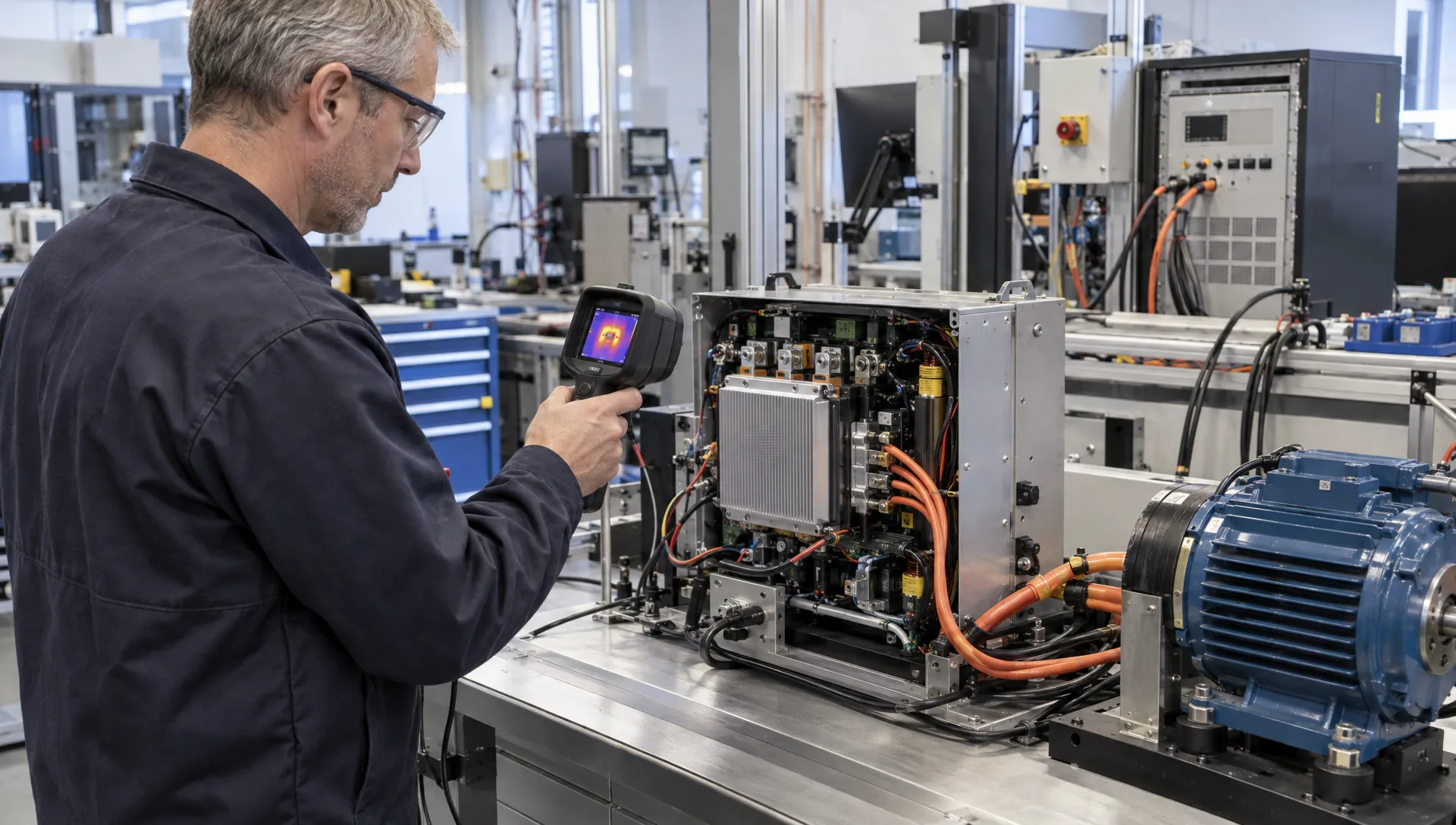
Test a representative assembly with its intended enclosure, mounting, cooling arrangement and nearby heat sources. Apply the relevant continuous load, duty cycles and credible overload conditions within a controlled test plan. Continue steady-load testing until temperatures stabilise rather than relying on a short demonstration.
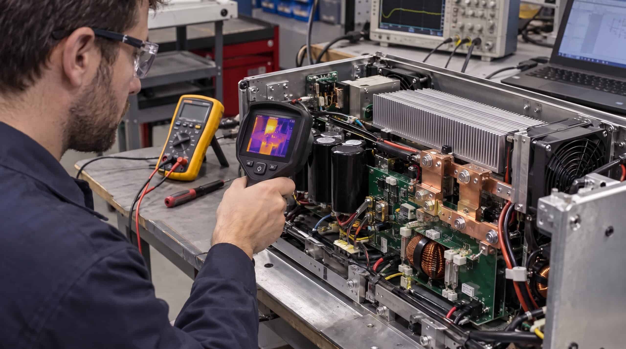
Measure voltage drop across critical sections to check resistance. Four-wire measurements help separate low conductor resistance from lead and contact resistance. Where possible, correlate those measurements with the actual fabrication evidence for the tested boards.
Thermal measurements need similar care. Infrared readings from shiny copper can be misleading because of emissivity and reflections. Suitable thermocouples or controlled-emissivity measurement areas can improve confidence, provided they do not materially alter the thermal behaviour.
Check bottlenecks individually, not just the hottest component or the centre of a copper pour. Record ambient temperature, operating mode, cooling conditions and measurement uncertainty so the result can be interpreted later.
Finally, assess the interaction with embedded firmware. Current limiting, overload timing and temperature monitoring affect the applied load profile, but they cannot compensate for an inadequately sized conductor under normal operation. Hardware paths and software protection behaviour should be verified together, including relevant fault responses.
Frequently asked questions
Does 2 oz copper carry twice the current of 1 oz copper? No. At the same finished width and length, doubling thickness approximately halves DC resistance. Current capacity also depends on heat removal and allowable temperature rise, so it does not automatically double.
Is nominal copper weight the same as minimum finished thickness? No. In pcb board making, a copper-weight designation must be clarified as starting foil or finished copper. Minimum acceptable thickness and the inspection basis should be agreed explicitly with the fabricator.
Can a trace-width calculator establish a safe current rating? It can support an initial estimate if its underlying method and assumptions are understood. Product release also needs assessment of finished geometry, temperature limits, installation conditions, bottlenecks and representative test results.
Does thicker copper improve EMC compliance? Not by itself. It can reduce resistive losses, but emissions and immunity also depend on switching behaviour, loop geometry, return paths, filtering and enclosure integration. Compliance must be assessed at product level.
Connect PCB fabrication choices to product reliability
ProMicro combines power electronics, analogue electronics, embedded systems and firmware expertise with PCB design, system engineering, enclosure design, prototyping and volume manufacturing support.
For a current-carrying PCB, that broader approach helps connect copper specifications with thermal behaviour, protection functions, EMC considerations and manufacturing readiness. If your design depends on assumptions about finished copper or conductor temperature, discuss the electrical and manufacturing requirements with ProMicro before committing them to a production release.