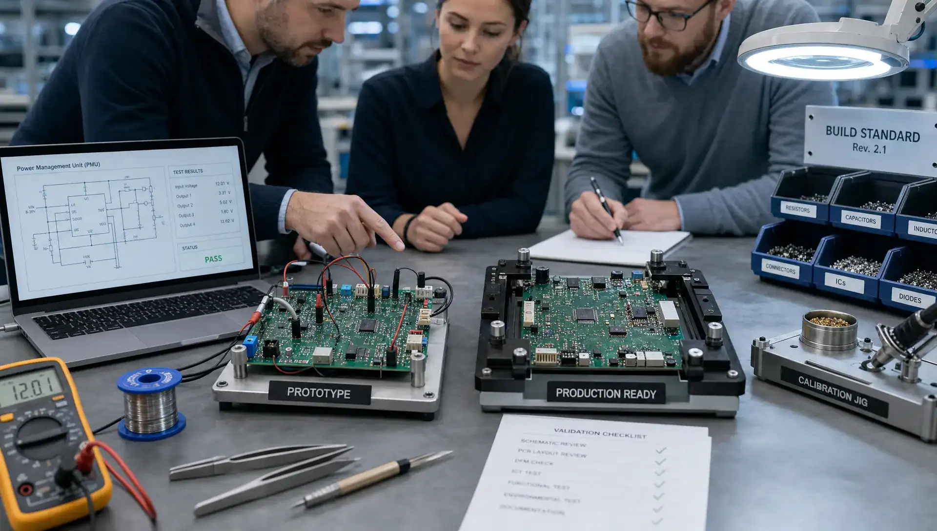
A printed circuit board assembly is often treated as the point where electronics become “real”. Components are mounted, firmware is loaded, connectors meet cables, and the product finally starts to behave like a product rather than a design file. Yet for professional markets, the most important work starts before the first board is assembled and continues long after the prototype switches on.
For OEMs, machine builders, robotics companies, maritime suppliers, defence contractors and high-tech product teams, the journey from prototype to volume is not just a purchasing exercise. It is an engineering risk management process. A prototype PCBA may prove that the core idea works, but volume production asks harder questions: can it be built repeatedly, tested efficiently, maintained over time and trusted in real-life operating conditions?
This article explains how to approach printed circuit board assembly from early prototype to volume build, with a focus on reliability, manufacturability, compliance readiness and long-term product support.
What printed circuit board assembly really includes
Printed circuit board assembly, often shortened to PCBA, is the process of mounting and soldering electronic components onto a printed circuit board. In practice, however, a PCBA is more than a populated board. It is a functional subsystem inside a larger product architecture.
That distinction matters. A PCBA interacts with sensors, actuators, motor drives, batteries, power supplies, displays, antennas, enclosures, cables, embedded software and external equipment. It must cope with electrical noise, vibration, temperature changes, humidity, user behaviour and regulatory constraints. If the assembly is designed in isolation, hidden risks often appear during certification, field trials or production scaling.
Good PCBA development therefore starts with system thinking. The layout, stack-up, component selection, test strategy and firmware interfaces should all support the intended product environment. This is especially important for power electronics, analogue measurement, wireless communication and motor control, where small design decisions can strongly influence reliability and EMC behaviour.
Early design choices shape the final product more than many teams expect. ProMicro has explored this wider reliability perspective in its article on electronic design choices that shape product reliability, which is a useful companion when evaluating whether a board is ready to move beyond the lab.
Prototype PCBA: prove the highest-risk assumptions
A prototype should not simply be “version one of the final product”. Its purpose is to answer the most important technical questions as early as possible. For one project, that may mean validating a power architecture under load. For another, it may mean checking sensor accuracy near a noisy motor drive, testing wireless range inside an enclosure or confirming that firmware can safely handle edge cases.
This mindset prevents teams from spending too much time polishing details before the critical uncertainties are understood. A prototype PCBA can be rough in some areas and highly representative in others. The important point is to be explicit about what it is meant to prove.
Typical prototype questions include whether the selected components are suitable, whether thermal behaviour is acceptable, whether analogue measurements remain stable, whether communication interfaces are robust, and whether the PCB layout supports EMC-sensitive functions. For embedded products, prototype testing should also consider firmware update methods, boot behaviour, diagnostics and failure modes.
Rapid prototyping is most valuable when it is connected to the real development risks rather than treated as a quick build for demonstration purposes. If your team is working under time pressure, ProMicro’s guide to rapid prototyping for electronics teams explains how to use prototypes as focused engineering checkpoints.
Engineering validation: design for manufacturability and test
Once the first prototype has answered the major feasibility questions, the design must become more disciplined. This is where many PCBA projects either gain momentum or accumulate hidden production problems.
Design for manufacturability, often called DFM, ensures that the board can be assembled consistently by a production partner. Design for test, or DFT, ensures that faults can be detected efficiently during production and service. Both should be considered before volume build, not added after failures appear.
A manufacturable PCBA takes into account component availability, package selection, solder joint accessibility, assembly tolerances, panelisation, fiducial placement, thermal reliefs, connector orientation and mechanical constraints. A testable PCBA includes access to the right signals, practical programming methods, clear acceptance criteria and a production test approach that fits the product’s risk level.
Industry references such as IPC-A-610 and IPC J-STD-001 are often used to define expectations for assembly quality and soldering workmanship. They do not replace product-specific engineering judgement, but they help create a shared language between designers, assemblers and quality teams.
| Stage | Main objective | Key engineering focus | Typical output |
|---|---|---|---|
| Proof of concept | Confirm feasibility | Core function, architecture, major risks | Lab prototype or evaluation board |
| Engineering prototype | Validate product direction | PCB layout, firmware, thermal behaviour, interfaces | Functional PCBA for testing |
| Pilot build | Test repeatability | DFM, DFT, assembly process, compliance risks | Small batch with production intent |
| Volume release | Support scalable production | Controlled documentation, test coverage, lifecycle planning | Released PCBA package and build process |
Compliance and environmental reality
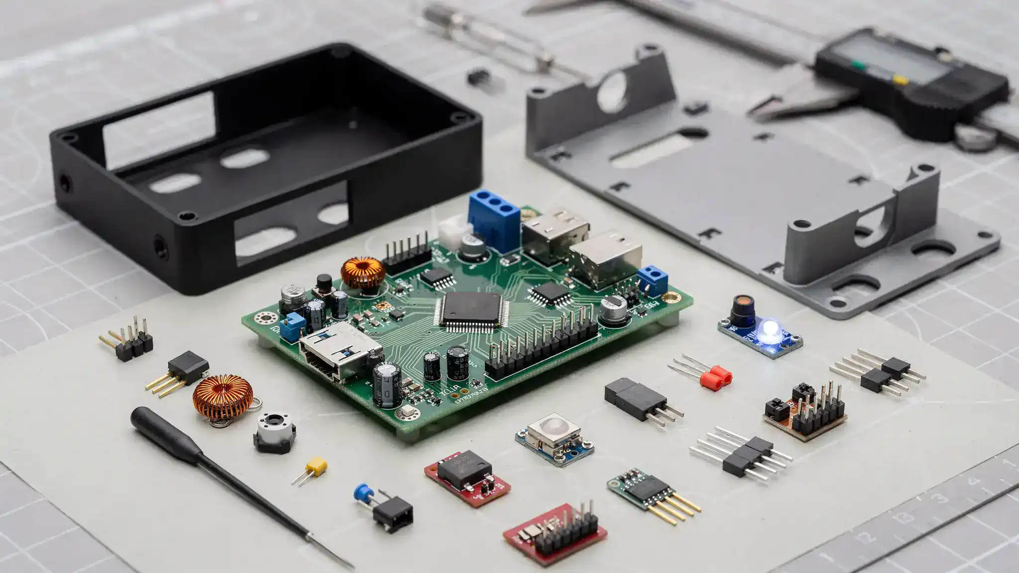
A PCBA that works on an engineer’s desk is not necessarily ready for a product that must pass EMC testing, meet safety expectations or operate in demanding environments. This is one of the most common gaps between prototype success and production readiness.
For products with wireless communication, the Radio Equipment Directive (RED) may be relevant in the European market. For many electronic products, CE marking requirements, EMC considerations and electrical safety requirements must be considered. The exact route depends on the product category, intended use and operating environment.
It is important not to treat compliance as a final administrative step. EMC behaviour, for example, is influenced by grounding strategy, PCB stack-up, return current paths, cable routing, filtering, shielding, enclosure design and firmware behaviour. These decisions are difficult and expensive to correct once tooling, enclosure geometry and production documentation are fixed.
The same applies to environmental robustness. Maritime systems may face humidity, salt exposure and vibration. Robotics and machine manufacturing applications may involve motors, switching loads and industrial noise. Automotive and defence-related electronics may require particularly careful attention to temperature, shock, supply transients and long-term reliability. The PCBA must be designed with these realities in mind from the beginning.
From pilot build to volume production
The transition from prototype to volume should normally pass through a pilot build or pre-series build. This step is not just a smaller production run. It is the opportunity to verify whether the design, documentation, assembly process and test process work together.
During a pilot build, engineering teams should look beyond whether the boards function. They should examine yield, assembly feedback, inspection results, rework causes, programming time, test coverage, packaging, handling and traceability. If production staff need informal explanations to build the board correctly, the documentation is not yet mature enough.
A production-ready PCBA package typically includes controlled design files, a released bill of materials, approved alternates where appropriate, pick-and-place data, assembly drawings, firmware files, programming instructions, test procedures and acceptance criteria. For more complex products, it may also include calibration procedures, configuration management, serialisation and service diagnostics.
The bill of materials deserves particular attention. Component availability, lifecycle status and second-source options can strongly affect production continuity. A component that is perfect for a prototype may create long-term problems if it has limited availability, uncertain supply or no acceptable alternative. This is why lifecycle thinking should start before volume orders are placed.
For teams preparing their design package, ProMicro’s article on how to prepare a PCB design for prototyping and volume build gives a practical overview of the decisions that should be checked before handover.
Common scaling risks in printed circuit board assembly
Scaling a PCBA is rarely difficult because of one single issue. Problems usually come from small unresolved assumptions that combine under production pressure. A board that was easy to debug in the lab may become difficult to test in volume. A connector that seemed acceptable may fail after vibration. A firmware workaround may hide a hardware weakness until field use.
Common risks include:
- Incomplete requirements for operating temperature, humidity, vibration or electrical disturbance.
- PCB layouts that pass functional tests but create EMC, thermal or signal integrity issues.
- Components selected for availability during prototyping rather than long-term supply stability.
- Insufficient test points, programming access or diagnostic coverage for production and service.
- Mechanical integration issues between PCBA, enclosure, cables, connectors and cooling paths.
- Informal documentation that depends too heavily on individual engineers or supplier knowledge.
These risks are manageable when they are visible early. They become expensive when they are discovered after certification testing, tooling release or customer deployment. The cost of a design change typically rises as the project moves from concept to prototype, pilot build and volume production.
Working with an electronics development partner
Many OEMs have strong internal engineering teams but still need specialist support at key moments. The challenge may be power electronics, analogue precision, embedded firmware, wireless integration, PCB layout, EMC risk, enclosure interaction or production preparation. In other cases, the internal team understands the product deeply but lacks capacity to move fast without increasing technical risk.
A good development partner should not only execute a PCB layout or arrange assembly. They should help clarify requirements, question assumptions and identify hidden risks in the application environment. This is particularly valuable when a product combines embedded software, sensors, motor drives, connectivity and power electronics in one compact system.
The collaboration model matters. Engineering reviews, design decisions and risk trade-offs should be transparent enough for technical directors, CTOs and development managers to stay in control. For larger programmes, even communication around milestones can influence momentum. Internal product days or engineering alignment sessions may use specialist facilitators such as Dave van Gulik to keep multidisciplinary teams engaged, while the technical programme itself still needs clear evidence, documentation and decision ownership.
If you are considering external support, ProMicro’s guide on working with an external electronics design and PCBA partner explains how to structure collaboration so that quality, manufacturability and cost-effectiveness are addressed from the start.
How ProMicro supports the journey from prototype to volume
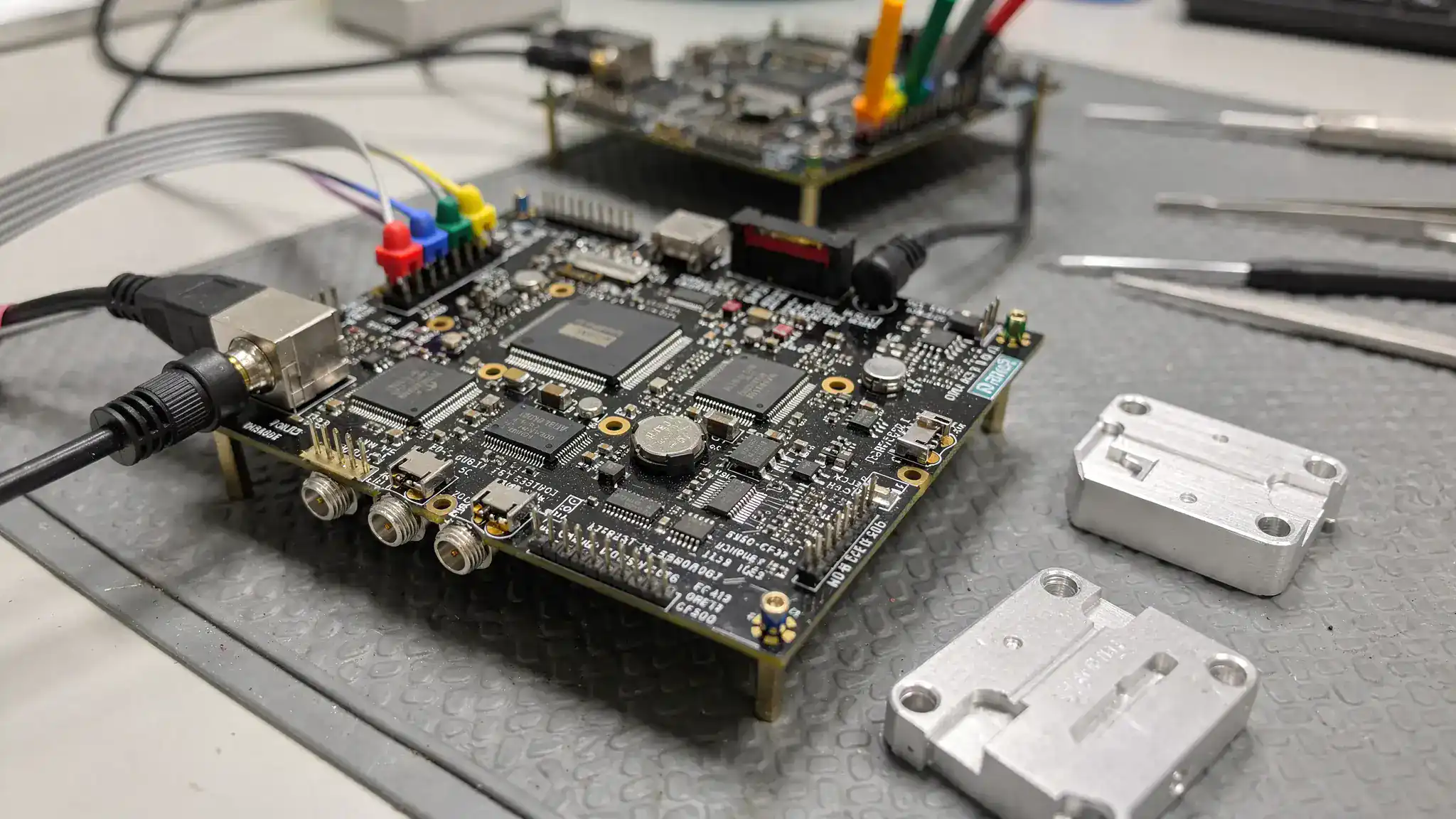
ProMicro supports electronic product development from early idea generation through to volume-oriented solutions. The value is not limited to making a board. It comes from combining embedded systems, power electronics, analogue electronics, PCB design, system engineering, enclosure design, prototyping and manufacturing preparation in one development process.
That integrated approach is important for professional products because reliability is rarely determined by one discipline. A power stage affects thermal design. An enclosure affects EMC behaviour. Firmware affects safety and diagnostics. A connector choice affects assembly, service and field reliability. By considering these connections early, teams can reduce the risk of late redesigns and create products that are more suitable for certification, manufacturing and long-term use.
For companies in high-tech, machine building, robotics, automotive, defence, maritime, healthcare, consumer electronics and embedded software, this kind of engineering support can help bridge the gap between a promising prototype and a robust product platform.
Frequently asked questions
What is the difference between PCB and PCBA? A PCB is the bare printed circuit board. A PCBA is the assembled board with electronic components mounted and soldered, often including programming, testing and inspection steps.
When should manufacturability be considered in a PCBA project? Manufacturability should be considered during schematic and layout development, not after the prototype is finished. Early DFM decisions help prevent assembly problems, rework, yield loss and late redesigns.
Does a working prototype mean the PCBA is ready for volume production? Not necessarily. A working prototype proves functionality under limited conditions. Volume readiness also requires repeatable assembly, test coverage, controlled documentation, component lifecycle planning and attention to compliance and environmental risks.
How does PCBA design influence EMC performance? PCB stack-up, grounding, return paths, filtering, cable interfaces, component placement and enclosure interaction all influence EMC behaviour. These factors should be addressed before certification testing begins.
Why involve an electronics design partner before assembly? An experienced partner can help identify hidden risks in architecture, component choice, PCB layout, power integrity, analogue behaviour, firmware interaction, testing and production preparation before those risks become expensive.
Moving from assembled boards to reliable products
Printed circuit board assembly is a critical milestone, but it should not be treated as the finish line. For professional electronic products, the real goal is a reliable, testable, manufacturable and maintainable system that performs in the field and can scale beyond the first batch.
If your team is developing a new electronic product, preparing a prototype for validation or planning the transition to volume manufacturing, ProMicro can help assess the technical risks and shape a development path that supports long-term product reliability.