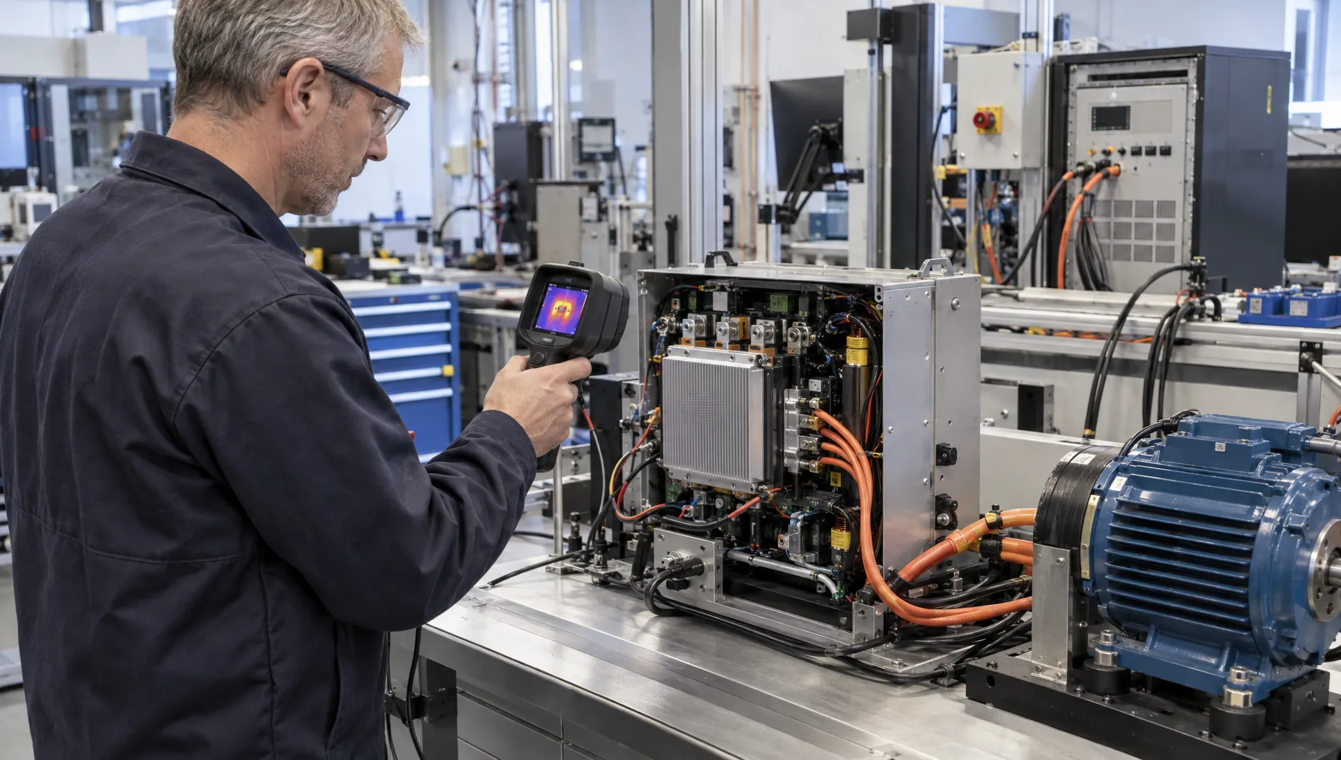
Derating electronic circuit board components means deliberately limiting their electrical and thermal stress below the relevant ratings. Done properly, it creates margin for supply variation, manufacturing tolerances, temperature changes and ageing. Done poorly, it becomes a blanket percentage that looks reassuring but misses the conditions that cause failures.
For professional embedded systems, motor drives and industrial equipment, the objective is not simply to specify larger components. It is to establish defensible operating limits, check them against the application and preserve those margins from prototype through volume production.
Define the operating envelope before choosing components
Start with the conditions the finished product will experience, rather than the nominal values on the schematic. A 24 V input does not establish the maximum voltage across every device. Supply tolerance, cable inductance, regenerative energy and switching overshoot can all change that stress.
The operating envelope should describe normal operation, start-up, shutdown, foreseeable overloads and relevant fault conditions. Include the temperature inside the enclosure, cooling restrictions, altitude where relevant and the expected load profile. An intermittently operated actuator and a continuously loaded drive require different thermal assessments.
For each critical component, identify both sustained stress and short-duration peaks. Record assumptions about firmware behaviour, protection thresholds and operating duty cycle. A software current limit should not be treated as an independent hardware protection mechanism unless the system architecture justifies that assumption.
When derating electronic circuit board components, use the worst credible combination of conditions, not an arbitrary combination of every possible maximum. Document which conditions can occur together and which are mutually exclusive. This keeps the analysis conservative without creating unnecessary cost or size.
Distinguish absolute maximum ratings from design limits
An absolute maximum rating is not a recommended operating point. Staying below it does not establish correct operation, adequate lifetime or an acceptable margin against transients.
Read the recommended operating conditions, electrical characteristics and rating notes alongside the absolute maximum table. A current rating may depend on case temperature or a specified PCB. A pulse rating may apply only to a particular duration and repetition rate. Several headline maxima may not be permissible simultaneously.
Define an internal design ceiling for each relevant stress. For voltage, a useful worksheet calculation is:
Voltage utilisation = worst-case applied voltage ÷ applicable voltage rating.
For power, the denominator should be the allowable power at the relevant temperature and mounting conditions, not automatically the headline wattage. For junction temperature, use an explicit temperature ceiling and temperature margin rather than a percentage of degrees Celsius.
A policy for electronic circuit board components should identify the component technology, applicable rating, design ceiling and evidence needed to demonstrate compliance. Customer-specified standards take precedence where applicable. NASA’s Electronic Parts and Packaging programme provides parts-assurance references, but aerospace requirements should not be copied into industrial products without considering their scope and assumptions.
How to derate electronic circuit board components by component type
Different technologies have different limiting mechanisms. The following checks provide a starting point for a component-level review, not universal acceptance limits.
| Component family | Stresses to assess | Constraint easily missed |
|---|---|---|
| Resistors | Continuous power, working voltage and pulse energy | Allowable power falls with temperature |
| Capacitors | Voltage, ripple current and temperature | Effective capacitance or endurance may limit suitability |
| MOSFETs and diodes | Voltage peaks, current, losses and junction temperature | Safe operating area and transient behaviour |
| Integrated circuits | Supply and pin voltages, dissipation and junction temperature | Power sequencing and injection-current limits |
| Inductors and transformers | Peak current, RMS current, temperature and insulation stress | Saturation and winding losses are separate constraints |
| Connectors | Contact current, voltage and temperature rise | Simultaneously loaded contacts and installation conditions |
Resistors and capacitors
For a resistor, check continuous dissipation against its temperature-dependent power curve. Working voltage is a separate limit: a high-resistance device can remain below its wattage rating while exceeding its permitted voltage. Repetitive pulses also require pulse-load data, not just an average-power calculation.
Capacitors require technology-specific treatment. Class II ceramic capacitance can decrease under DC bias and vary with temperature and ageing. Aluminium electrolytic suitability depends on ripple heating, temperature and the manufacturer’s endurance data. Tantalum devices need particular attention to surge conditions and the manufacturer’s application guidance.
Derating electronic circuit board components must therefore preserve circuit function as well as reduce stress. A ceramic capacitor with adequate voltage margin may still provide too little effective capacitance for converter stability, filtering or hold-up requirements.
Semiconductors and integrated circuits
For a MOSFET, assess drain-source voltage peaks, gate-source excursions, conduction losses and switching losses. Use temperature-appropriate resistance data. Check the safe operating area for start-up, current limiting and fault clearing, especially when the device operates in its linear region.
A pulsed current rating does not establish suitability for repeated overloads. Its stated conditions may assume a low initial temperature or a pulse duration unlike the application. Likewise, avalanche capability should not be treated as an unrestricted substitute for controlling switching transients.
For diodes, consider forward losses, reverse voltage and reverse-recovery behaviour where relevant. For ICs, review pin-level stresses as well as the supply rail. An externally driven input can violate injection-current limits when the IC is unpowered, even though its normal operating voltage is acceptable.
These checks connect hardware selection with firmware sequencing, protection timing and system interfaces. They cannot be completed from the bill of materials alone.
Magnetics and connectors
An inductor’s saturation-current rating and thermal-current rating describe different constraints. Check peak current against the permitted inductance reduction and RMS current against temperature rise. Manufacturer definitions vary, so compare the underlying test conditions rather than only the current figures.
For transformers, include core flux, winding losses, insulation requirements and temperature. For connectors, examine contact resistance, ambient temperature, the number of loaded contacts and the specified wire or PCB termination.
Reliable derating of electronic circuit board components also requires installation assumptions to remain valid. A connector tested with particular conductors or limited contact loading may need a different assessment when many adjacent contacts carry current inside a warm enclosure.
Work through electrical and thermal examples
The following examples use hypothetical project limits and component characteristics. They demonstrate the method, not recommended derating percentages for every design.
Example 1: voltage margin on a switched 24 V rail
Assume a nominal 24 V supply has a maximum positive tolerance of 10%. The maximum steady voltage is therefore 26.4 V. Circuit analysis and representative measurements identify a further 8 V switching overshoot, giving a worst-case peak of 34.4 V.
For a 40 V MOSFET, voltage utilisation is:
34.4 V ÷ 40 V = 86%.
If the project has adopted an illustrative 75% voltage-utilisation ceiling, the required rating is at least:
34.4 V ÷ 0.75 = 45.9 V.
A 60 V candidate clears that particular voltage check. It still needs assessment for losses, gate drive, safe operating area and temperature. Alternatively, reducing overshoot through layout or a suitable clamp may improve margin without increasing the device rating.
The value of derating electronic circuit board components lies in this traceable decision: measured or calculated stress is compared with a defined limit. The selected voltage class alone is not evidence of reliability.
Example 2: resistor power at elevated temperature
Assume a resistor is rated at 0.5 W up to 70 °C, with allowable power falling linearly to zero at 155 °C. At a temperature of 105 °C, measured or defined as required by its datasheet, the allowable power is:
0.5 W × (155 − 105) ÷ (155 − 70) = 0.294 W.
If the resistor dissipates 0.20 W, utilisation is approximately 68% of the temperature-adjusted rating, not the 40% suggested by comparing against 0.5 W.
If the project additionally permits only 60% of that adjusted rating, its design ceiling becomes approximately 0.176 W. The component does not meet that project criterion.
Possible responses include reducing dissipation, changing package or resistor technology, improving the thermal environment or selecting a more suitable rating. Apply the replacement’s own curve rather than assuming its behaviour scales directly with nominal wattage. Also confirm whether the manufacturer’s curve uses ambient, terminal or another defined temperature.
Example 3: IC junction-temperature margin
A first-order estimate can be written as:
Junction temperature ≈ local ambient temperature + dissipated power × junction-to-ambient thermal resistance.
With a local ambient of 70 °C, dissipation of 0.8 W and an assumed thermal resistance of 45 °C/W, the estimate is 106 °C. Against an illustrative project ceiling of 110 °C, only 4 °C of margin remains.
However, datasheet junction-to-ambient values depend strongly on the test board and environment. Texas Instruments’ guide to semiconductor and IC package thermal metrics explains why these values need careful interpretation and distinguishes thermal resistance from characterisation parameters.
Thermal derating of electronic circuit board components should therefore use calculations as a starting point, followed by evidence representative of the enclosure, PCB and airflow. Where uncertainty is significant, a small calculated margin is not a robust acceptance basis. Transient loads may also require transient thermal analysis rather than a steady-state estimate.
Verify margins on representative hardware
Build a derating worksheet before prototype testing. For each critical part, record the exact manufacturer part number, datasheet revision, stress parameter, worst-case value, applicable rating, project ceiling and utilisation or temperature margin. Add the source of evidence and the conditions under which it applies.
Verification should target assumptions most likely to change the result:
- Supply extremes combined with the relevant maximum load and enclosure temperature.
- Start-up, shutdown, load steps and protection activation, including their repetition rates.
- Component tolerances and protection thresholds that increase stress.
- Restricted cooling or other foreseeable operating conditions identified by the requirements and risk analysis.
Measure switching peaks with an appropriate probe and connection method. A long probe ground lead can introduce ringing that obscures the actual stress. Temperature measurements also need interpretation: a package-surface measurement is not automatically the junction temperature.
When validating electronic circuit board components, reconcile measured results with the model. If a peak or hotspot is higher than predicted, investigate the cause before accepting the design on the basis that it remains below an absolute maximum.
Board construction and placement affect these results. ProMicro’s explanation of circuit board design decisions that shape reliability provides broader context for the layout and thermal assumptions behind the component calculations.
Preserve derating margins through production and lifecycle changes
A successful prototype does not freeze component stress. Alternative parts, PCB changes, enclosure revisions and firmware updates can alter the operating conditions established during development.
Define the characteristics an alternative component must preserve. For a capacitor, nominal capacitance and voltage are insufficient: effective capacitance, ESR, ripple capability and temperature characteristics may matter. For a MOSFET, check losses, gate charge, safe operating area and package thermal behaviour, not just current and voltage ratings.
Reassess affected margins after changes to switching frequency, current limits, protection delays or operating duty cycle. Component derating and firmware configuration should be controlled together when software determines hardware stress.
The evidence for derating electronic circuit board components should remain part of the product’s controlled design record. Include unresolved assumptions, acceptance criteria and the tests required when a substitution changes critical characteristics.
This discipline complements PCB assembly and manufacturing preparation for reliable electronics. It gives procurement and manufacturing teams a technical basis for substitutions rather than relying on nominal equivalence.
Derating also has limits. It does not replace insulation coordination, EMC assessment, fault protection or qualification testing, and it does not by itself demonstrate conformity with applicable legislation or standards.
Frequently asked questions
Is there a universal derating percentage? No. Suitable limits depend on component technology, manufacturer guidance, operating conditions, failure consequences and applicable customer or sector requirements. Use documented component-specific criteria rather than applying one percentage to voltage, current, power and temperature.
Does selecting a higher-rated part always improve reliability? Not necessarily. A higher voltage rating may change switching losses, capacitance, package size or cost. Compare the complete operating behaviour and failure risks, not just the headline rating.
How should electronic circuit board components be assessed for short pulses? Check the manufacturer’s pulse-load, safe-operating-area or transient thermal data as appropriate. Include pulse duration, repetition rate and initial temperature. Average power alone can miss excessive instantaneous stress.
Can derating predict product lifetime? Derating supports lifetime objectives, but it does not establish a universal life multiplier. Lifetime claims need a failure-mechanism-specific model, suitable manufacturer data and validation relevant to the application’s operating profile.
When should the analysis be reviewed? Establish it during component selection and update it after layout, prototype measurements and relevant design changes. Review affected calculations before approving component substitutions or releasing firmware that changes electrical or thermal stress.
Make component margins part of the development process
A useful derating review produces clear decisions: which parts have adequate margin, which assumptions require testing and which design changes are needed before release.
ProMicro supports integrated electronics development, combining power electronics, analogue design, embedded systems, PCB design and prototyping with manufacturing and lifecycle support. For projects with demanding operating conditions, that integrated approach helps connect component calculations with firmware behaviour, mechanical integration and compliance-aware design, rather than treating the PCB as an isolated deliverable.