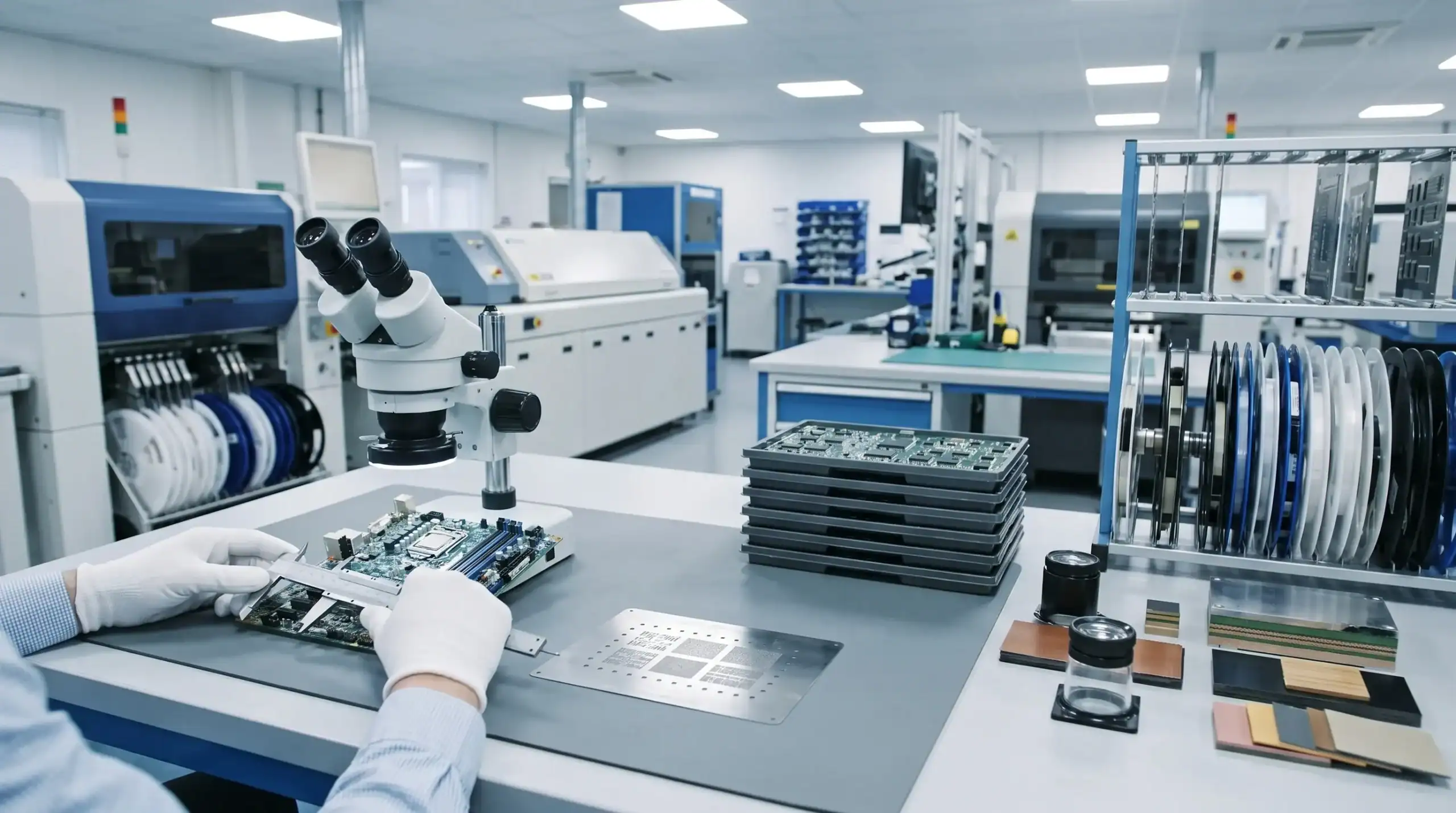
When a product fails in the field, the root cause is often traced back to decisions made much earlier than final test. Material selection, stack-up control, component handling, soldering process, inspection strategy and supplier change control all influence whether a PCB assembly performs reliably over time.
For engineering managers and technical directors, PCB fab and assembly choices should therefore be treated as product quality decisions, not only purchasing decisions. A low unit price can be attractive in a spreadsheet, but the real cost appears when a product suffers from intermittent faults, EMC problems, moisture ingress, production rework or lifecycle instability.
In sectors such as machine manufacturing, robotics, maritime, automotive, defence and high-tech equipment, the PCB is rarely a simple carrier for components. It is part of the electrical, thermal, mechanical and regulatory behaviour of the full product. The fabrication and assembly route must reflect that reality.
Why fabrication and assembly decisions affect more than the board
A PCB can pass a basic continuity check and still be unsuitable for the product it will enter. Quality depends on how the board behaves under voltage, load, temperature, vibration, humidity, contamination, software-driven switching patterns and long-term component ageing.
This is why final inspection alone cannot create product quality. Inspection can detect visible defects, but it cannot recover design margin that was lost through poor material choice, uncontrolled impedance, insufficient creepage, weak thermal design or inadequate test access. The most reliable products are built from decisions that align design intent, fabrication capability and assembly process control from the beginning.
For example, a motor drive board may require copper thickness, thermal vias and isolation distances that are very different from a low-power sensor node. A wireless IoT device may depend heavily on stack-up repeatability, ground reference quality and antenna keep-out discipline. A maritime product may need stronger attention to corrosion, conformal coating compatibility and connector sealing. These choices sit between electronics design, manufacturing engineering and application knowledge.
This is also why PCB quality should be considered alongside broader electronic design choices that shape product reliability, including power integrity, analogue performance, EMC behaviour and lifecycle support.
Start with product requirements, not only a Gerber package
Many quality problems begin when PCB fabrication and assembly are requested from incomplete documentation. Gerber files describe copper and mechanical layers, but they do not fully describe the product context. A manufacturer may be able to build what is drawn, yet still not understand the environmental, regulatory or functional margins the product needs.
A stronger procurement package includes fabrication drawings, stack-up requirements, material expectations, copper weights, surface finish, controlled impedance needs, assembly drawings, BOM status, approved alternatives, inspection criteria and test requirements. For professional products, it should also clarify whether the build is a prototype, engineering validation batch, pilot run or volume release.
| Decision area | Why it affects quality | Evidence to request or define |
|---|---|---|
| Application environment | Drives material, coating, connector and corrosion choices | Temperature, humidity, vibration and ingress requirements |
| Electrical performance | Influences stack-up, impedance, grounding and isolation | Power levels, switching frequencies, RF paths and safety distances |
| Production volume | Determines how much process automation and test coverage are needed | Prototype, pilot and expected annual volume |
| Compliance context | Affects layout, filtering, shielding and documentation discipline | EMC, RED, CE and safety-related assumptions |
| Lifecycle expectations | Reduces risk from obsolete or uncontrolled components | Approved BOM, second sources and change control process |
The earlier these requirements are made explicit, the easier it becomes to choose a fabrication and assembly route that supports the product rather than simply producing boards.
Fabrication choices that influence board reliability
PCB fabrication quality starts with the laminate and stack-up. FR-4 is not a single material with one performance level. Glass transition temperature, dielectric behaviour, comparative tracking index, thermal conductivity and moisture absorption can all matter depending on the application. High-current, high-temperature or high-frequency designs may need tighter material control than a generic board quote provides.
Copper thickness is another common source of misunderstanding. Thicker copper can improve current handling and thermal spreading, but it also affects track width, spacing, etching tolerances and assembly solderability. For power electronics, the copper strategy must be aligned with thermal modelling, connector selection, creepage and mechanical constraints.
Stack-up control is particularly important for EMC-sensitive, high-speed and RF designs. Layer order, reference planes, dielectric thickness and return current paths influence signal integrity and emissions. A substitution that looks harmless from a procurement perspective can change impedance or coupling behaviour enough to affect test results.
Vias also deserve close attention. Aspect ratio, plating thickness, via-in-pad treatment, thermal via patterns and annular ring tolerances can influence both manufacturability and field reliability. In products exposed to thermal cycling or vibration, weak via construction may become an intermittent fault long after the prototype stage.
Surface finish should be selected for the component technology, storage conditions, soldering process and lifecycle expectations. ENIG, HASL, OSP and immersion finishes each have practical trade-offs. The right answer depends on fine-pitch assembly, shelf life, flatness needs, lead-free soldering and potential rework.
| Fabrication choice | Potential quality risk if poorly specified | Typical engineering consideration |
|---|---|---|
| Laminate material | Warping, moisture sensitivity or thermal instability | Temperature range, power dissipation and environment |
| Stack-up | EMC issues, impedance variation or poor return paths | Layer order, plane continuity and dielectric control |
| Copper weight | Excessive heating or manufacturing tolerance problems | Current density, thermal design and etching capability |
| Via construction | Intermittent faults or fatigue under thermal cycling | Aspect ratio, plating quality and via placement |
| Surface finish | Solderability issues, poor flatness or storage problems | Component pitch, shelf life and assembly process |
| Solder mask definition | Shorts, leakage paths or poor coating adhesion | Clearances, mask dams and contamination control |
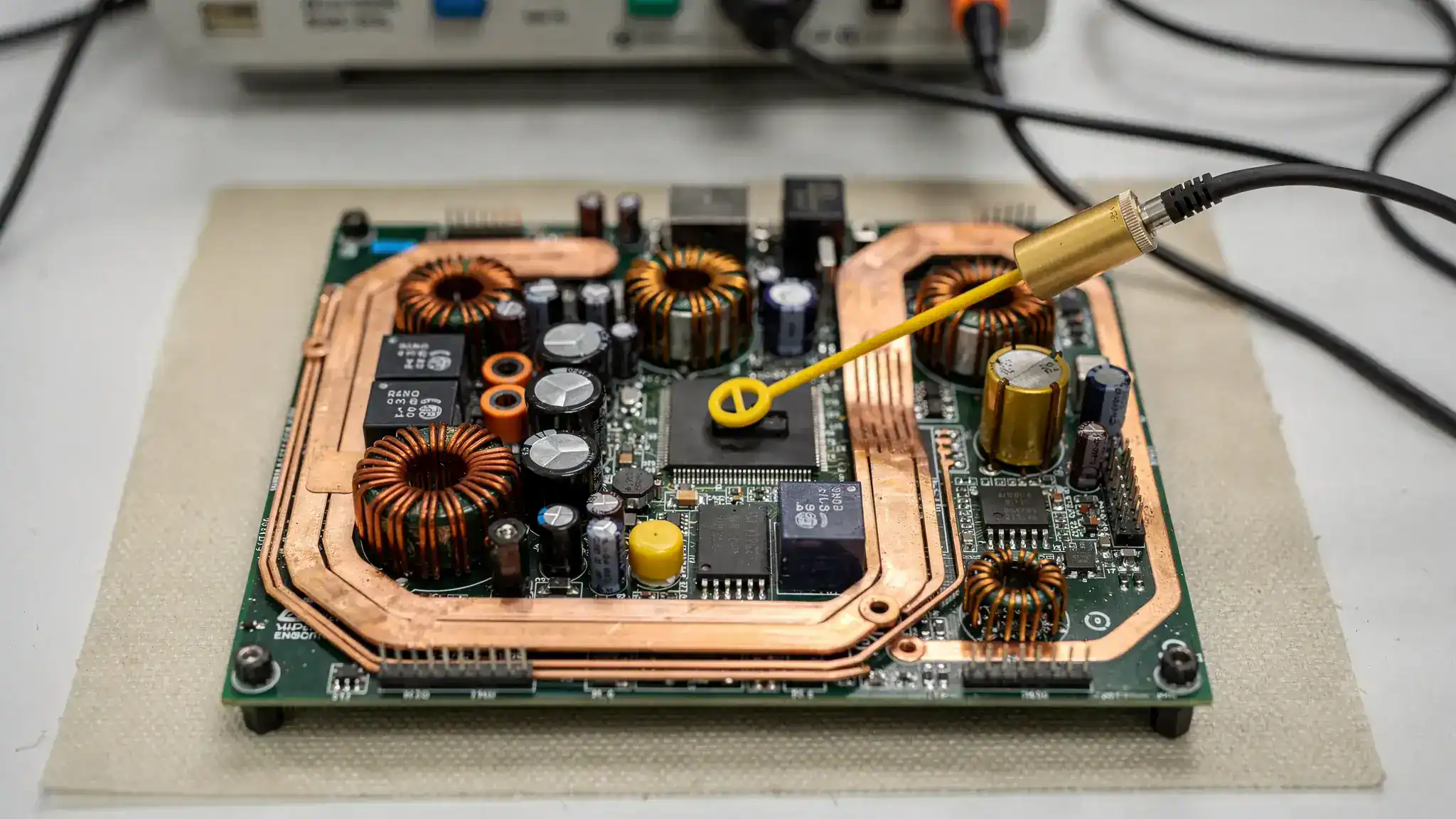
Assembly choices that affect field performance
Assembly quality starts before the first component is placed. The BOM should be checked for availability, lifecycle status, package suitability, moisture sensitivity level and approved alternates. Uncontrolled substitutions can change thermal behaviour, EMC performance, analogue accuracy or safety margin, even when the part appears electrically equivalent.
Stencil design and solder paste selection are equally important. Aperture reductions, paste type, board thickness, component density and thermal mass influence solder joint quality. Fine-pitch ICs, QFNs, BGAs, large connectors and power components may each require different process attention. A generic stencil strategy can create insufficient solder, tombstoning, voiding or bridging.
The reflow profile should match the actual board, not only the paste datasheet. Dense assemblies with mixed thermal mass need profiling to avoid cold joints on large components or overheating of sensitive parts. Selective soldering, wave soldering and hand soldering also require process control, especially around connectors, through-hole power components and heat-sensitive devices.
Cleaning and residue control are often underestimated. No-clean flux does not mean residues are irrelevant in every environment. High impedance analogue circuits, sensor interfaces, high voltage sections and humid operating conditions may be sensitive to ionic contamination. Coating or potting over residues can lock in a long-term reliability risk.
Inspection strategy should match component technology and product risk. AOI can catch many placement and solder defects, but hidden joints under BGAs, QFNs and certain power packages may require X-ray inspection. Functional testing, boundary scan, in-circuit testing or dedicated test fixtures may be needed when visual inspection cannot confirm real product behaviour.
For teams planning a new build, it is worth reviewing how assembly PCB planning that prevents costly rework connects component selection, documentation, test strategy and manufacturability before production pressure increases.
Supplier capability and process control matter as much as price
A capable PCB fabricator or assembler does more than accept files and ship boards. They control materials, document processes, manage deviations and communicate risks before they become production failures. Price is important, but it should be evaluated alongside process maturity and evidence of control.
Relevant quality references include IPC-A-600 for acceptability of printed boards, IPC-6012 for qualification and performance of rigid printed boards, IPC-A-610 for acceptability of electronic assemblies and J-STD-001 for soldered electrical and electronic assemblies. Not every product needs the same class or inspection level, but the agreed standard should be clear before production starts.
Traceability is also critical. For professional and long-life products, teams should be able to trace board batches, material certificates, solder paste lots, component lots, reflow profiles, inspection results and deviations. Without traceability, recurring faults become much harder to investigate and contain.
Facility discipline matters too. ESD control, humidity control, storage conditions, chemical handling, cleanliness and safe remediation procedures all reduce avoidable contamination and downtime. In manufacturing environments where water damage, mould, demolition dust or hazardous materials could affect equipment or stock, it is sensible to involve licensed environmental remediation teams rather than treating these risks as ordinary housekeeping.
The best supplier relationships are transparent about limitations. If a fabricator cannot hold a requested tolerance consistently, or an assembler sees a layout that will create soldering defects, that information should surface before the build. Silence is not a quality process.
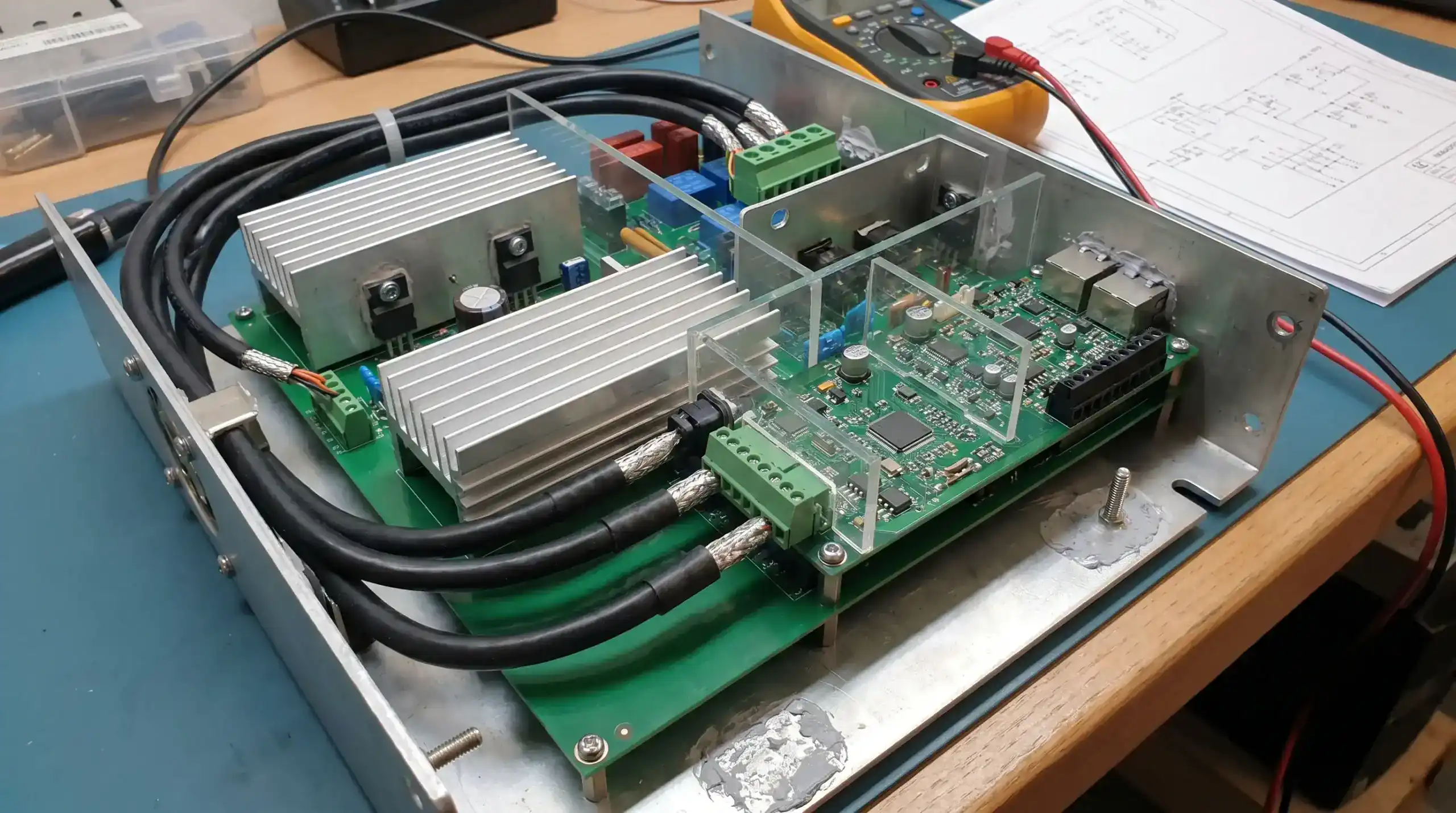
Prototype, pilot and volume builds should not be treated the same
A prototype is often built to answer engineering questions quickly. It may include manual rework, hand-soldered modifications or components that are convenient rather than final. That can be appropriate during early development, but it becomes dangerous when a prototype is mistaken for a production-ready design.
Pilot builds are the bridge between engineering validation and volume production. They reveal whether the layout, BOM, test process, documentation and supplier capability can produce repeatable results. A pilot build should not only ask whether the board works. It should ask whether the board can be built, inspected, tested and repaired consistently.
Volume production then requires tighter change control. Component alternatives, panelisation changes, process modifications and test fixture updates should be assessed before implementation. Even small changes can affect EMC, thermal behaviour, firmware timing, sensor accuracy or mechanical fit.
| Build stage | Main objective | Quality focus |
|---|---|---|
| Prototype | Validate concept and core functions | Fast learning, design corrections and risk discovery |
| Engineering validation | Confirm electrical, thermal and mechanical behaviour | Measurement, stress testing and compliance preparation |
| Pilot build | Prove repeatable manufacturing process | DFM, DFT, inspection coverage and supplier feedback |
| Volume production | Deliver stable products over time | Traceability, change control and lifecycle management |
A practical way to reduce risk is to consider production constraints while the design is still flexible. ProMicro’s guidance on preparing a PCB design for prototyping and volume build explains why early requirements, architecture review and testability are so important.
Hidden quality risks that often appear too late
Some PCB quality risks are easy to miss because they do not appear during a simple bench test. They emerge during EMC testing, thermal stress, field operation, supply chain changes or scaling to higher volumes.
Common examples include:
- Choosing a low-cost fabrication route without confirming stack-up repeatability or material equivalence.
- Using minimum track and spacing rules everywhere, leaving no process or contamination margin.
- Placing high-current switching paths near sensitive analogue or RF circuits.
- Leaving too few test points for production diagnostics and field failure analysis.
- Allowing component substitutions without reviewing firmware, thermal, EMC and safety implications.
- Treating conformal coating as a late add-on instead of checking masking, residues and connector compatibility.
- Designing panelisation after layout release, then discovering handling, depanelisation or fixture problems.
- Failing to define acceptance criteria for cosmetic, soldering, dimensional and functional issues.
The cost of these issues increases sharply as the product moves from prototype to certification and volume manufacturing. Early prevention is usually less expensive than late correction, especially when tooling, enclosure design, firmware validation and customer commitments are already in place.
How to make better PCB fab and assembly decisions
Good decisions come from connecting design intent with manufacturing reality. That means involving electronics design, embedded software, mechanical design, procurement, quality and manufacturing stakeholders before the board is released. It also means asking suppliers for technical feedback, not only quotations.
For complex products, the PCB should be reviewed as part of a system. Power electronics, analogue front ends, sensors, wireless communication, motor drives, connectors, enclosure constraints and firmware behaviour all interact. A board that is easy to assemble but difficult to test is not production-ready. A board that works in the lab but radiates during EMC testing is not mature. A board that relies on one soon-to-be-obsolete component is not lifecycle-ready.
A structured review should consider whether the design has enough electrical margin, thermal margin, mechanical robustness, documentation clarity and test access. It should also challenge assumptions about user behaviour and field conditions. Products for maritime, robotics, automotive, defence and industrial equipment often encounter stresses that are not visible in early lab demonstrations.
This is where an end-to-end electronics development partner can add value. ProMicro supports embedded systems, power electronics, analogue electronics, PCB design, prototyping and preparation for volume manufacturing. The aim is not only to create a board, but to help create electronics that are reliable, manufacturable, maintainable and suitable for the real product environment.
Frequently asked questions
What is the difference between PCB fabrication and PCB assembly? PCB fabrication creates the bare printed circuit board, including layers, copper, vias, solder mask and finish. PCB assembly places and solders components onto that board, then inspects and tests the resulting assembly.
Why do PCB fab and assembly choices affect product quality? They determine whether the design can be built consistently and survive real operating conditions. Material selection, stack-up, soldering process, inspection, test access and traceability all influence reliability.
Is the lowest-cost PCB supplier always a risk? Not always, but price should not be evaluated alone. The right supplier must match the product’s technical requirements, process controls, documentation needs, compliance context and lifecycle expectations.
When should DFM and DFT reviews happen? They should happen before layout release and again before pilot production. Early reviews make it easier to improve manufacturability, test coverage and assembly yield without expensive redesign.
Can a prototype PCB be used directly for volume production? Sometimes, but it should not be assumed. A production-ready assembly needs controlled documentation, stable components, repeatable processes, inspection criteria, test strategy and change control.
Build product quality into the PCB, not around it
PCB quality is not created by one supplier, one inspection step or one final test. It is the result of connected decisions across electronics design, fabrication, assembly, testing, compliance preparation and lifecycle management.
If your team is developing a complex electronic product and wants to reduce risks before prototyping, certification or volume production, ProMicro can help assess the design choices that matter. From embedded systems and power electronics to PCB design, prototyping and manufacturing preparation, the focus is on building reliable electronics that are ready for real-world use.