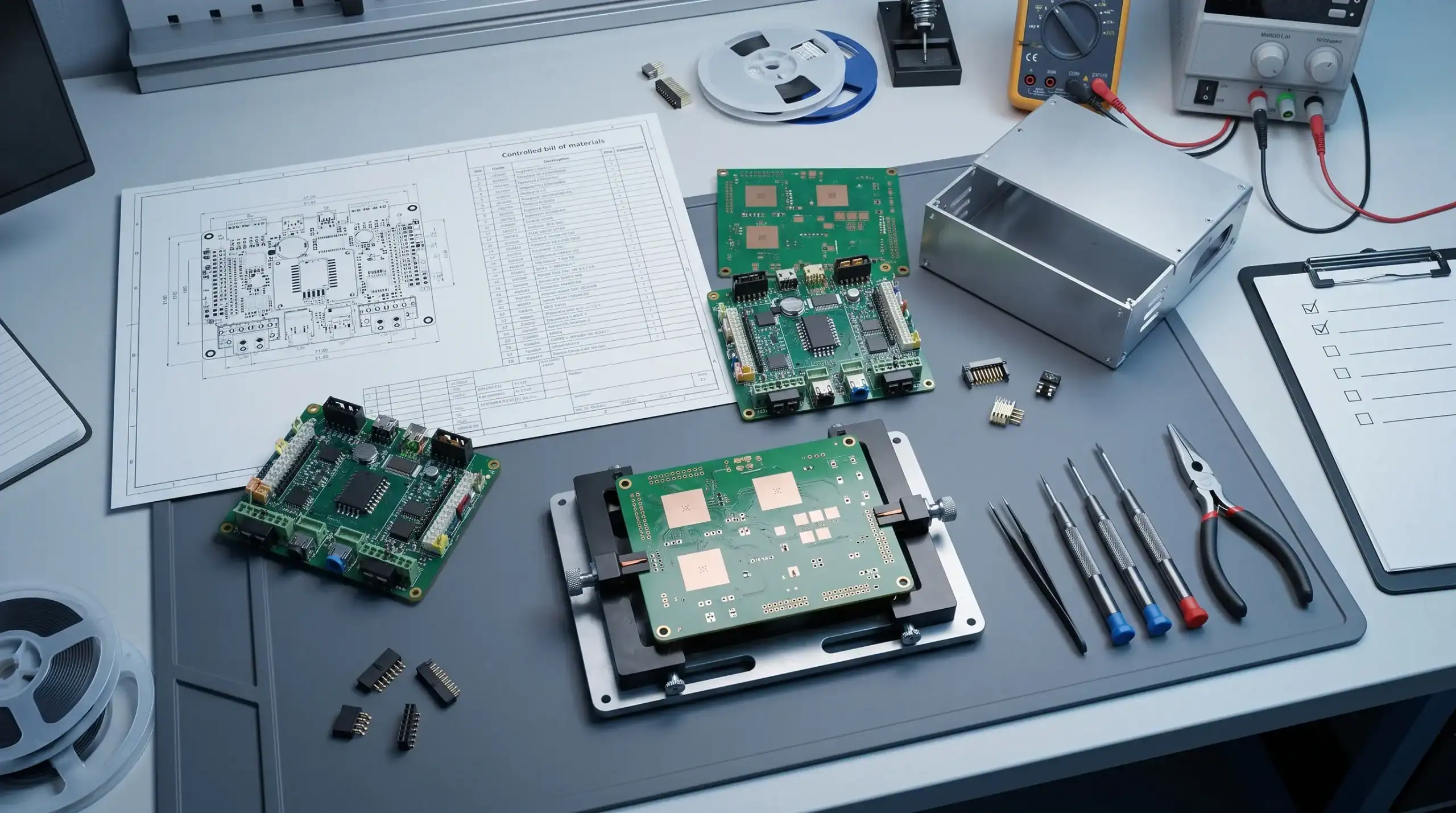
Costly PCB rework rarely begins on the assembly line. It usually starts earlier, when requirements are incomplete, the bill of materials is treated as purchasing admin, test access is forgotten, or mechanical constraints are not considered until the enclosure arrives.
For engineering managers, CTOs and product owners in sectors such as high-tech machinery, maritime, robotics, automotive and defence, assembly PCB planning is not a minor production detail. It is a risk-control activity. Done well, it protects schedules, certification work, product reliability and long-term maintainability. Done late, it turns every design change into a queue of respins, manual modifications and difficult conversations with suppliers.
The goal is not simply to make a board that can be assembled. The goal is to make a board that can be assembled repeatedly, tested confidently, integrated into the product, supported over its lifecycle and scaled without hidden surprises.
Why PCB assembly rework becomes so expensive
A solder bridge or misplaced component is visible. A weak planning process is not. That is what makes it more dangerous. By the time a board reaches assembly, many decisions have already become expensive to change: component packages, connector positions, thermal paths, test access, clearances, firmware programming method and even enclosure interfaces.
Rework has obvious costs, such as labour, replacement components, delayed builds and scrap. But for professional electronics, the indirect costs are often larger. Manual rework can introduce variability between units. Late layout changes can invalidate EMC assumptions. A component substitution can affect thermal performance, safety margins or radio behaviour. A test point that is missing from the first batch may slow every future production unit.
In regulated or demanding environments, rework can also disrupt compliance planning. A prototype that works in the lab may still fail when exposed to vibration, conducted noise, radiated emissions, temperature cycling or inconsistent field power. When those risks are only discovered after assembly, the project loses both time and design freedom.
Start with the requirements the assembled PCB must prove
Good PCB assembly planning begins before schematic capture. The first question is not which components fit on the board. It is what the assembled board must prove in the final product.
For example, a motor drive in a robot arm has different assembly priorities than a low-power IoT sensor, even if both use microcontrollers, sensors and connectors. The motor drive may demand careful current paths, thermal management, isolation, creepage and EMC containment. The sensor product may place more emphasis on antenna performance, battery life, enclosure effects and programming logistics.
Requirements should cover the real operating context, not only the intended function. That includes supply voltage range, peak currents, expected temperature, humidity, vibration, cable lengths, maintenance access, cleaning processes, enclosure constraints, regulatory targets and expected production volume.
| Planning area | Question to answer before assembly | Rework risk reduced |
|---|---|---|
| Operating environment | What temperature, vibration, moisture and electrical disturbances will the product face? | Late component changes, coating changes and mechanical redesign |
| Power behaviour | What are the worst-case current, inrush, dissipation and fault conditions? | Overheated tracks, undersized components and unreliable protection |
| Connectivity | Which cables, antennas, sensors and external interfaces affect layout and assembly? | Connector relocation, EMC problems and enclosure conflicts |
| Test strategy | How will each assembled board be programmed, measured and accepted? | Manual debugging, inaccessible signals and slow production testing |
| Lifecycle | How long must the product remain buildable and serviceable? | Obsolete components, uncontrolled substitutions and redesigns |
When these questions are answered early, the PCB design can be aligned with manufacturing, testing and compliance expectations from the start. If they are left open, the assembly process becomes the first moment when the product is forced to confront reality.
Bring assembly constraints into schematic and layout decisions
PCB assembly planning is often mistaken for a task that happens after layout. In practice, assembly constraints should influence the schematic, the component selection and the PCB layout.
Component package selection is a good example. A very small package may look attractive for density, but it can complicate inspection, rework, test access and supply chain flexibility. A high-current connector may satisfy the datasheet rating, but still need board-level reinforcement, thermal relief, strain management and clearance from sensitive analogue circuitry. A switching regulator may be electrically correct, but poor placement can create noise problems that are expensive to fix later.
Important assembly-related design choices include fiducials, component orientation, panelisation, solder mask clearances, stencil considerations, placement keep-outs, access for automated optical inspection, programming connector access and spacing around heat-generating parts. For mixed-signal, power or wireless products, layout also has to support EMC and signal integrity goals, not merely physical assembly.
If your team is still defining release data and layout rules, ProMicro’s guide on how to prepare a PCB design for prototyping and volume build provides a useful wider view of design readiness before manufacturing.
Industry standards such as IPC-A-610 and IPC J-STD-001 are often used to define workmanship and soldering expectations. They do not replace product-specific engineering judgement, but they help create a shared language between design teams, assembly partners and quality teams.
Treat the BOM as an engineering document
The bill of materials is not just a purchasing list. It is part of the design intent. If the BOM is weak, assembly becomes vulnerable to delays, substitutions and performance drift.
A mature BOM should identify manufacturer part numbers, approved alternatives, package details, tolerance, temperature rating, voltage rating, moisture sensitivity where relevant, lifecycle status and any compliance-sensitive properties. For safety-related, radio, automotive, maritime or defence-adjacent products, traceability and controlled alternatives may be just as important as unit price.
Component availability should be checked before the design is frozen. This is especially important for embedded systems, power electronics and analogue designs, where a substitute can change timing, noise, thermal behaviour or calibration. A passive component may seem interchangeable until its voltage coefficient, dielectric type or tolerance affects a measurement circuit. A MOSFET may meet headline current ratings but behave differently under switching losses, gate drive conditions or thermal constraints.
The BOM should also reflect the expected lifecycle. A prototype can tolerate a temporary workaround. A production-ready product cannot depend on components that are already near end-of-life, single-sourced without justification, or difficult to procure in the required quantities.
Design for test before the first build
If a board cannot be tested efficiently, every assembly issue becomes harder to diagnose. Design for test is therefore one of the strongest ways to prevent rework.
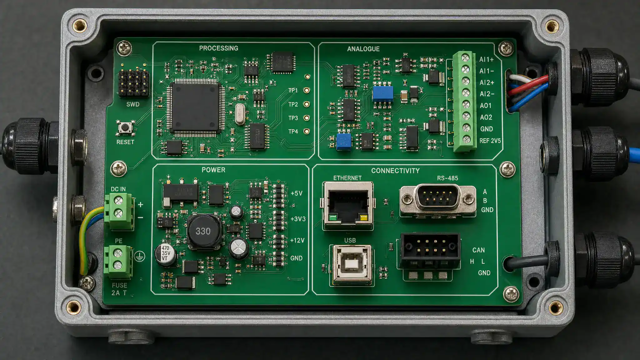
Test planning starts with deciding what the assembled PCB must demonstrate at each stage. During bring-up, engineers may need access to rails, clocks, reset lines, communication buses, analogue references, programming interfaces and safety circuits. During production, the test should be repeatable, fast enough for the build volume and clear enough to separate assembly defects from design issues.
For embedded systems, the programming and configuration method should be planned before layout release. Will the unit be programmed through a connector, pads, a bed-of-nails fixture or a wireless process? Is there a secure boot or calibration step? Can the firmware identify hardware revisions? Can the product record serial numbers, test results or configuration data where required?
For power electronics, test planning must also consider safe energisation. Current limits, load conditions, thermal observation and fault response should be controlled. A power board that is first tested only at full load invites avoidable damage.
The same discipline continues after assembly. ProMicro’s article on how an assembled circuit board becomes production-ready explains why controlled bring-up, functional testing and production preparation are essential steps between a populated board and a reliable product.
Use prototypes to answer the highest-risk questions
A prototype build should not simply prove that the CAD files can produce a board. It should answer the technical questions that carry the most risk.
For one project, the highest risk may be thermal performance under peak load. For another, it may be antenna performance inside the enclosure, EMC emissions from a motor drive, sensor accuracy in a noisy environment, or the reliability of a connector exposed to vibration. The assembly plan should define these learning objectives before the prototype is ordered.
This prevents a common failure mode: building a beautiful prototype that does not generate enough evidence. If no one planned the test points, load conditions, firmware hooks or measurement procedure, the team may need another board revision just to collect the data that the first prototype should have delivered.
| Prototype decision | Good planning choice | What it prevents |
|---|---|---|
| Build quantity | Order enough units for electrical, firmware, mechanical and destructive tests where needed | One prototype becoming a bottleneck for every discipline |
| Test access | Include pads, headers or fixture access for critical signals | Slow debugging and avoidable layout respins |
| Variant strategy | Build controlled variants for uncertain components or configurations | Unstructured experiments and unclear conclusions |
| Mechanical integration | Check connector positions, enclosure fit and cable routing during the prototype stage | Late enclosure changes and assembly interference |
| Compliance learning | Use pre-compliance measurements where practical | Discovering EMC or radio risks only at formal testing |
Well-planned rapid prototyping gives the team a reality check while there is still time to adjust the design without derailing the full product plan.
Prepare assembly documentation as a controlled handover
Many rework problems are caused by unclear handovers. A fabricator, assembly house, test engineer or firmware developer should not have to infer critical design intent from scattered files and informal messages.
A mature assembly pack typically includes:
- PCB fabrication data, such as Gerber, drill files, ODB++ or IPC-2581 where applicable.
- Pick-and-place files with clear component orientation.
- A controlled BOM with approved alternatives and do-not-fit information.
- Assembly drawings showing polarity, mechanical constraints and special instructions.
- Stencil, solder paste, coating or cleaning requirements where relevant.
- Programming files, firmware version information and configuration instructions.
- Functional test procedure, acceptance criteria and inspection requirements.
- Revision history that makes engineering changes visible and traceable.
This level of planning is not unique to electronics. In construction and fit-out work, experienced premium renovation contractors in Dubai reduce rework by aligning drawings, materials, sequencing and acceptance criteria before work starts. PCB assembly follows the same practical principle: ambiguity at handover becomes cost at execution.
For technical products, controlled documentation also supports future maintenance. When a product returns from the field, or when a new production batch is started months later, the team needs to know exactly which design revision, firmware version, component alternatives and assembly instructions were used.
Make compliance and manufacturability visible before volume
Compliance should not be treated as a final gate at the end of development. For products that involve power electronics, wireless communication, sensors, motor drives or long cable interfaces, EMC, RED, CE and safety-related considerations can influence architecture, layout, enclosure design, firmware behaviour and test strategy.
Planning with compliance in mind does not guarantee certification success. It does, however, reduce the likelihood that avoidable design choices will create late failures. Examples include poor segregation between noisy and sensitive circuits, inadequate grounding strategy, insufficient filtering at external interfaces, unclear antenna placement, weak thermal margins or missing protective circuitry.
Manufacturability must be considered in the same way. A prototype may be hand-assembled successfully, but volume production needs repeatability. Component spacing, inspection access, panel handling, fixture design, coating processes and connector assembly all affect whether the product can scale. The earlier these details are visible, the easier they are to solve without major redesign.
This is where system-level thinking matters. The PCB is not isolated from firmware, cables, sensors, enclosure, user behaviour or the installation environment. A board that is electrically correct but mechanically awkward, difficult to test or sensitive to cable routing is still not production-ready.
Warning signs that your PCB assembly planning is immature
Rework risk is often visible before the first board is built, if the team knows what to look for. The following signs suggest that assembly planning needs more attention before release:
- The BOM contains generic parts, unresolved alternates or components with uncertain availability.
- Test points are added only after layout, instead of being designed around the test strategy.
- The enclosure, connectors and cable routing have not been checked against the PCB assembly.
- Firmware programming and calibration are not defined for production units.
- EMC or safety requirements are discussed only after prototype assembly.
- The assembly partner receives files without clear drawings, revision control or acceptance criteria.
- The prototype build has no written plan for what must be measured, stressed or learned.
None of these issues means the project is failing. They simply indicate that design decisions are not yet mature enough for a low-risk assembly handover. Addressing them early is far cheaper than correcting them after boards have been built.
How ProMicro approaches assembly PCB planning
For complex electronic products, PCB assembly planning is strongest when it is connected to the full development process. That includes system engineering, embedded software, power and analogue electronics, PCB layout, enclosure considerations, prototyping, test planning and preparation for volume manufacturing.
ProMicro supports customers across these connected disciplines. The value is not only in producing a PCB design, but in helping teams identify hidden technical risks before they become rework, certification delays or production problems. This is especially relevant when internal engineering teams need extra capacity, specialist knowledge or an external partner who can challenge assumptions constructively.
A good planning process makes requirements explicit, captures design intent, reduces ambiguity for suppliers and keeps the product’s real operating environment in focus. It also creates a clearer route from first idea to production-ready electronics.
Frequently asked questions
What is assembly PCB planning? Assembly PCB planning is the process of preparing a PCB design, BOM, documentation, test strategy and manufacturing handover so the board can be assembled, tested and scaled with minimal rework.
When should PCB assembly planning start? It should start before schematic design. Requirements, component choices, test access, mechanical constraints and compliance targets all influence whether the assembled PCB will be reliable and manufacturable.
Why do prototypes still need assembly planning? Prototypes are most valuable when they answer specific technical risks. Without planning, a prototype may work visually but fail to provide the data needed for thermal, EMC, firmware, mechanical or production decisions.
Can good planning eliminate all PCB rework? No. Complex electronics development always involves learning and iteration. Good planning reduces avoidable rework by making risks visible earlier and by ensuring that assembly, testing and integration are considered before release.
What should be included in a PCB assembly handover pack? A strong handover pack usually includes fabrication data, pick-and-place files, a controlled BOM, assembly drawings, firmware and programming instructions, test procedures, inspection requirements and revision history.
Need a stronger route from PCB assembly planning to production?
If your product combines embedded software, power electronics, analogue circuitry, sensors, wireless communication or demanding real-world operating conditions, assembly planning should be part of the engineering strategy from day one.
ProMicro helps companies develop reliable electronic products from concept and prototyping through to production-ready solutions, with practical attention to manufacturability, testability, compliance risks and long-term lifecycle support.